


More Related Content
Similar to Advance Microprocessor application and its uses (20)
Recently uploaded (15)


Advance Microprocessor application and its uses
- 1. EEN 15252: MICROPROCESSOR & APPLICATIONS Lecture 07 & 08 Dr. Vishal Kumar Gaur
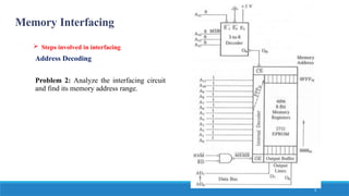
- 2. Memory Interfacing 2 ’āś Steps involved in interfacing Address Decoding Problem 2: Analyze the interfacing circuit and find its memory address range.
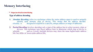
- 3. ’āś Steps involved in interfacing Type of address decoding 1. Absolute Decoding refers to a technique where the entire address space is used to uniquely identify each memory chip or device. This means that the address decoder circuitry is designed to respond to a specific, unique address or range of addresses. 2. Partial Decoding involves decoding only a part of the address bus to select memory chips or devices. This technique uses fewer address lines to determine which chip or device is selected, and as a result, multiple devices may share the same higher-order address bits but differ in lower-order address bits. 3 Memory Interfacing
- 4. ’āś Steps involved in interfacing Address Decoding: Partial Decoding Example Problem 3: Explain the decoding logic and memory address range for memory shown in interfacing circuit. Memory Interfacing 4
- 5. ’āś Steps involved in interfacing Address Decoding: Partial Decoding Example Problem 3: Explain the decoding logic and memory address range for memory shown in interfacing circuit. Initial Address Memory Interfacing A15 A14 A13 A12 A11 A10 A9 A8 A7 A6 A5 A4 A3 A2 A1 A0 0 0 1 0 0 x x x 0 0 0 0 0 0 0 0 5 0 0 1 0 0 x x x 1 1 1 1 1 1 1 1 Final Address
- 6. ’āś Steps involved in interfacing Address Decoding: Partial Decoding Example Problem 3: Explain the decoding logic and memory address range for memory shown in interfacing circuit. Initial Address 6 Memory Interfacing A15 A14 A13 A12 A11 A10 A9 A8 A7 A6 A5 A4 A3 A2 A1 A0 0 0 1 0 0 x x x 0 0 0 0 0 0 0 0 0 0 1 0 0 x x x 1 1 1 1 1 1 1 1 Final Address A10 A9 A8 0 0 0 0 0 1 0 1 0 0 1 1 1 0 0 1 0 1 1 1 0 1 1 1 Possible values of donŌĆÖt care pins
- 7. ’āś Steps involved in interfacing Address Decoding: Partial Decoding Example Problem 3: Explain the decoding logic and memory address range for memory shown in interfacing circuit. 7 Memory Interfacing A15 A14 A13 A12 A11 A10 A9 A8 A7 A6 A5 A4 A3 A2 A1 A0 0 0 1 0 0 x x x 0 0 0 0 0 0 0 0 0 0 1 0 0 x x x 1 1 1 1 1 1 1 1 Initial Address Final Address A10 A9 A8 Initial Address Final Address 0 0 0 2000H 20FFH 0 0 1 2100H 21FFH 0 1 0 2200H 22FFH 0 1 1 2300H 23FFH 1 0 0 2400H 24FFH 1 0 1 2500H 25FFH 1 1 0 2600H 26FFH 1 1 1 2700H 27FFH Possible values of donŌĆÖt care pins
- 8. Memory Interfacing 0 0 0 0 0 0 0 0 0 0 0 0 1 1 1 1 1 1 0 0 0 0 0 0 1 1 1 1 1 1 0 0 0 0 0 0 1 1 1 1 1 1 0 0 0 0 0 0 1 1 1 1 1 1 0 0 0 0 0 0 1 1 1 1 1 1 0 0 0 0 0 0 1 1 1 1 1 1 0 0 0 0 0 0 1 1 1 1 1 1 0 0 0 0 0 0 1 1 1 1 1 1 Address Range 2000H 20FFH 2100H 21FFH 2200H 22FF H 2300H 23FF H 2400H 24FFH 2500H 25FF H 2600H 26FFH 2700H 27FF H A10 A9 A8 A7 A6 X x x 0 0 0 0 0 0 0 1 1 0 0 1 0 0 1 1 0 1 0 0 0 1 1 0 1 1 0 0 1 1 1 0 0 0 0 1 1 1 0 1 0 0 1 1 1 1 0 0 0 1 1 1 1 1 0 0 1 1 A15 A14 A13 A12 A11 0 0 1 0 0 Register Select A5 A4 A3 A2 A1 A0 ’āś Steps involved in interfacing Address Decoding: Partial Decoding Example Chip Enable DonŌĆÖt care 1st Possible Range 2nd Possible Range 3rd Possible Range 4th Possible Range 5th Possible Range 6th Possible Range 7th Possible Range 8th Possible Range 8
- 9. ’āś Steps involved in interfacing Address Decoding: Partial Decoding Example 9 Memory Interfacing The memory chip of 256 Byte (256 memory registers) occupies the memory space of 2048 locations in 8085, eight times the space of its size. Some of the address lines of microprocessor left unused while designing address decoding circuit. Because of this multiple possible address ranges will be formed. If total memory space of 8085 is not required for the system then, this type of address decoding can be used. The advantage of this technique is fewer components are required for memory interfacing because of this board size reduces and in turn cost reduces.
- 10. ’āś Steps involved in interfacing Address Decoding Problem 04: Consider a system in which 32kB memory space is implemented using four numbers of 8kB memory. Interface the EPROM and RAM with 8085 processor. Instruction: The total memory capacity is 32kB. So, let two number of 8kB memory be ROM and the remaining two numbers be RAM. 10 Memory Interfacing
- 11. ’āś Steps involved in interfacing Memory Interfacing 1. The total memory capacity is 32kB. 2. So, let two number of 8kB memory be ROM and the remaining two numbers be RAM. 3. Each 8kB memory requires 13 address lines and so the address lines A0- A12 of the processor are connected to 13 address pins of all the memory. 4. The address lines and A13 - A14 can be decoded using a 2-to-4 decoder to generate four chips select signals. 5. These four chips select signals can be used to select one of the four memory IC at any one time. 6. The address line A15 is used as enable for decoder. The simplified schematic memory organization is shown CS RD WR A0-A12 4kB x 8 RAM 1 CS RD 4kB x 8 WR RAM 2 A0-A12 CS RD A0-A12 4kB x 8 ROM 1 CS RD A0-A12 4kB x 8 ROM 2 Decoder 3 2 1 0 X0 A15 8085 Data Data Data Data E X1 Y1 Y 0 Y3 Y2 AD7-AD0 WR IO/M RD 8-Bit D0-D7 ALE Latch E Address bus A14 A13 A12-A8 A0-A12 A0-A7 MEMR MEWR A8-A12 11
- 12. ’āś Steps involved in interfacing Memory Interfacing 8 kB RAM 1 8 kB RAM 2 8 kB ROM 1 8 kB ROM 2 CS RD WR A0-A12 4kB x 8 RAM 1 CS RD 4kB x 8 WR RAM 2 A0-A12 CS RD A0-A12 4kB x 8 ROM 1 CS RD A0-A12 4kB x 8 ROM 2 Decode r 3 2 1 0 A15 8085 Data Data Data Data E X1 X0 Y1 Y0 Y3 Y2 AD7-AD0 WR IO/M RD D0-D7 ALE 8-Bit Latch E Address bus A14 A13 A12-A8 A -A 0 12 A0-A7 MEMR MEWR A8-A12 12
- 13. Microprocessor: 8085 13 Instruction Format and Set
- 14. Microprocessor: 8085 14 Instruction Format and Set ’é¦ Instruction is a binary pattern designed to indicates a microprocessor to perform a specific function. ’é¦ Each instruction has two parts: one is the task to be performed, called the operation code (opcode), and the second is the data to be operand on, called the operand. ’é¦ The operand (or data) can be specified in various ways. It may include 8-bit (or 16-bit) data, an internal register, a memory location, or an 8-bit (or 16-bit) address. ’é¦ In some instructions, the operand is implicit. ’é¦ The entire group of instructions, called the instruction set, determines what functions the microprocessor can perform. ’é¦ 8085 microprocessor instructions can be classified into the following five functional categories: data transfer operations, arithmetic operations, logical operations, branching operations, and machine- control operations.
- 15. Microprocessor: 8085 Instruction Format and Set ’é¦ Instruction/Opcode Format ’é¦ Consider a single byte instruction available at memory location ŌĆśNŌĆÖ. ’é¦ The 8-bit of the op-code is divided into three portions. ’é¦ D2 D1 D0 when necessary contains the source code SSS. ’é¦ D2 D1 D0 group contains the code of destination register DDD. ’é¦ The first group D7 D6 gives the idea of the mnemonic of the operation code. N 15
- 16. Microprocessor: 8085 Instruction Format and Set ’é¦ In the design of 8085, all operations, registers, and status flags are identified with a specific code. ’é¦ For example, all internal registers are identified as follows: 16
- 17. Microprocessor: 8085 Instruction Format and Set ’é¦ An instruction to move the content of accumulator in register C. ’é¦ Move the content: 01 ’é¦ To register C: ’é¦ From register A: 001 (DDD) 111 (SSS) ’é¦ Binary instruction: 01001111 4FH N 17
- 18. Microprocessor: 8085 18 Instruction Set 8085 instruction set is classified based 1) on the word size, and 2) on the function performed.
- 19. Microprocessor: 8085 19 Instruction Set 8085 instruction set is classified into following three groups according to word size or byte size. 1) 1-byte instructions 2) 2-byte instructions 3) 3-byte instructions In 8085, terms ŌĆ£byteŌĆØ and ŌĆ£wordŌĆØ are synonymous because it is an 8-bit microprocessor.
- 20. Microprocessor: 8085 Instruction Set 1) 1-byte instructions: This type of instructions includes the opcode and the operand in the same byte. For example: ’é¦ These instructions are stored in 8-bit binary format in memory. 20
- 21. Microprocessor: 8085 ’é¦ These instructions would require two memory locations each to store the binary codes. N Instruction Set 2) 2-byte instructions: In this type of instructions, the first byte specifies the operation code and the second byte specifies the operand. For example: N N+1 N N+1 21
- 22. Microprocessor: 8085 Instruction Set 3) 3-byte instructions: In this type of instructions, the first byte specifies the operation code and the following two bytes specifies the 16-bit address. For example: N N+1 N+2 N N+1 N+2 ’é¦ These instructions would require three memory locations each to store the binary codes. 22
- 23. Microprocessor: 8085 23 Instruction Set ’é¦ Whenever a 2-byte instruction is used the first byte at memory location N is the op- code of the instruction followed by either an 8-bit data or an 8-bit address at memory location N+1. ’é¦ Whenever a 3-byte instruction is involved, the first byte at memory location N is the opcode followed by either a-16 bit address or a 16-bit data. The second memory location i.e., N+1 contains the lower order addresses or data and the third memory location N+2 contains the higher order address or data.
- 24. Microprocessor: 8085 24 Instruction Set 8085 instruction set is classified into following categories based on the the type of actions taken by the processor. 1) Data Transfer Instructions 2) Arithmetic Instructions 3) Logic and Bit Manipulation Instructions 4) Branch Instructions 5) Machine Control Instructions The 8085 microprocessor instruction set has 74 operation code that result in 246 instructions.
- 25. Microprocessor: 8085 25 Instruction Set 1) Data Transfer Instructions There are 15 such basic instructions and 86 variations. This group comprises instructions that move data between internal registers of Ø£ćØæØ, between internal register and external memory location and I/O transfer. One of the register is always located in the Ø£ćØæØ itself; the other may be located in one of the following: 1) An I/o device 2) Memory 3) The microprocessor (internal register) It means, this group of instructions includes transfer of data from internal register to another internal register, internal register to memory, memory to internal register, accumulator (A) to output device, or from input device to accumulator
- 26. Microprocessor: 8085 26 Instruction Set 1) Data Transfer Instructions Summary: These type of instructions perform the following six operations. ’é¦ Load an 8-bit number in a register ’é¦ Load an 16-bit number in a register pair ’é¦ Copy from register to register ’é¦ Copy between register and memory ’é¦ Copy between I/O and accumulator ’é¦ Copy between registers and stack memory
- 27. ’é¦ This instruction can have 49 variations (7x7), seven combinations for source registers (SSS) and seven combinations for destination registers (DDD) other than 110. MOV r1, M ’é¦ Move the content of the memory location whose address is available into (H,L) pair into the internal general purpose register r1ŌĆØ ’é¦ M(H,L) is the source register, (r1) is the destination register. ’é¦ It is a single byte instruction at memory location N. It has 7 variation as DDD can not be 110 because direct memory to memory data transfer is not allowed. ’é¦ The operation code is, Instruction Set 1)Data Transfer Instructions MOV r1, r2 ’é¦ This is a single byte instruction at memory location N. The opcode of the instruction will be Microprocessor: 8085 27
- 28. Instruction Set 1)Data Transfer Instructions MOV M, r1 ’é¦ Move the content of the internal general purpose register r into the memory location whose address is available in (H,L) register pair. ’é¦ It is a single byte instruction. The operation code is ’é¦ It has seven variations. SSS cannot be 110 because direct memory to memory data transfer is not allowed Microprocessor: 8085 28
- 29. Instruction Set 1)Data Transfer Instructions MVI r1, DATA ’é¦ DATA is the symbolic name given to 8-bit data which is immediately available as second byte of the instruction. ’é¦ Therefore, the source of data is the 2nd byte of the instruction itself. ’é¦ It is a 2 byte instruction (and has 7 variations) at the memory location N & N+1. The opcode of the instruction is MVI M, DATA ’é¦ Move 8-bit data available immediately as a 2nd byte of the instruction to the memory location whose address is available in memory pointed by (H, L) register pair. ’é¦ It is a 2 byte instruction (no variation) at the memory location N & N+1. The opcode of the instruction is 29 Microprocessor: 8085
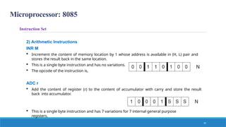
- 30. Microprocessor: 8085 30 Instruction Set 2) Arithmetic Instructions Instructions meant for arithmetic operations that add, subtract, increment or decrement data in a register are put in this group. Normally two operands are necessary for any arithmetic operation. One of the operand is always assumed to be available in accumulator. The other operand can be made available in one of the three locations: (a) In an internal general purpose register (r). (b) In a memory location pointed by M-pointer i.e., (H, L) pair. (c) Immediately in the instruction itself as a 2nd byte. The frequently used arithmetic operations are: ’é¦ Add ’é¦ Subtract ’é¦ Increment (Add 1) ’é¦ Decrement (Subtract 1)
- 31. Microprocessor: 8085 Instruction Set 2) Arithmetic Instructions ADD r ’é¦ Add the content of register (r) to the content of accumulator and store the result back into the accumulator. ’é¦ This is a single byte instruction. ’é¦ The opcode of the instruction is, ’é¦ It has 7 variations for 7 internal general purpose registers. ADD M ’é¦ ’é¦ This is a single byte instruction and has no variations. 31
- 32. Microprocessor: 8085 Instruction Set 2) Arithmetic Instructions ADD DATA ’é¦ Add the content available as the second byte of the instruction to the content of accumulation and store the result back into the accumulator. ’é¦ This is a single byte instruction and has no variations. ’é¦ The opcode of the instruction is, ADC r ’é¦ Add the content of register (r) to the content of accumulator with carry and store the result back into accumulator. ’é¦ This is a single byte instruction and has 7 variations for 7 internal general purpose registers. 32
- 33. Microprocessor: 8085 Instruction Set 2) Arithmetic Instructions INR M ’é¦ Increment the content of memory location by 1 whose address is available in (H, L) pair and stores the result back in the same location. ’é¦ This is a single byte instruction and has no variations. ’é¦ The opcode of the instruction is, ADC r ’é¦ Add the content of register (r) to the content of accumulator with carry and store the result back into accumulator. ’é¦ This is a single byte instruction and has 7 variations for 7 internal general purpose registers. 33
- 34. Microprocessor: 8085 34 Instruction Set 3) Logic and Bit Manipulation Instructions ’é¦ Instructions that carry out logic operation, such as AND, OR, EX-OR, compare data in the accumulator with another internal or external register, complement and rotate data in the accumulator are considered in this group. The frequently used operations are: ’é¦ AND ’é¦ OR ’é¦ XOR ’é¦ Compare, Rotate Bits
- 35. Microprocessor: 8085 Instruction Set 3) Logic and Bit Manipulation Instructions ANA r ’é¦ AND bit by bit the content of register (r) to the content of accumulator and store the result back in the accumulator ’é¦ This is a single byte instruction. ’é¦ The opcode of the instruction is, ANI DATA ’é¦ AND bit by bit the content available as a second byte of instruction to the content of the accumulator and store the result back in the accumulator. ’é¦ This is a two byte instruction and has no variations. ’é¦ The opcode of the instruction is, 35
- 36. Microprocessor: 8085 36 Instruction Set 4) Branch Instructions ’é¦ This group of instructions is used to alter the normal sequential program flow and force the program to proceed from a different point. ’é¦ Branch instructions can be of two types: conditional & unconditional. ’é¦ Unconditional branch instructions simply cause the program to branch to the indicated instruction whenever these instructions are encountered, i.e., (PC) is loaded with a new address. ’é¦ Conditional branch instructions examine the status of one of the four processor flags (Z, CY, P, S) to determine if the specified branch instruction is to be executed. If the condition tested is TRUE, it causes a branching to occur otherwise not. ’é¦ Condition flags are not affected by any instruction in this group only program counter (PC) is affected. ’é¦ AC is not used for specifying condition. The 8 conditions that are tested are given below:
- 37. Microprocessor: 8085 Instruction Set 4) Branch Instructions ’é¦ AC is not used for specifying condition. The 8 conditions that are tested are given below: 37
- 38. Microprocessor: 8085 Instruction Set 4) Branch Instructions Jcond ADDR ’é¦ There are 8 conditions that can be checked. They are JNZ, JZ, JNC, JC, JPO, JPE, JP, and JM. ’é¦ So, there are 8 variations for this instruction. ’é¦ The I6-bit address in the (PC) just at the end of the instruction depends upon the condition to be tested. (PC) will be loaded with B3B2 if the given condition is TRUE, otherwise (PC) will go to (PC)i+3. Figure: Flow chart for conditional jump instruction 38 Figure: Operation code format of instruction
- 39. Microprocessor: 8085 Instruction Set 4) Branch Instructions JMP ADDR ’é¦ ADDR is the symbolic name given to the 16- bit address data available as the 2nd and 3rd ’é¦ bytes of the instruction. ’é¦ Load the PC with the 16- bit address data available in the instruction itself as the 2nd and 3rd bytes of instruction so that the next instruction is fetched from this address in the succeeding instruction cycle. ’é¦ This is a three byte instruction. 39
- 40. Microprocessor: 8085 Instruction Set 5) Machine Control Instructions EI (Enable Interrupts) ’é¦ The interrupt system is disabled just after RESET operation. ’é¦ There is an internal INTE F/F (interrupt enable flip-flop) which is reset in RESET operation. ’é¦ It is a single byte instruction. ’é¦ The interrupt system is enabled using EI instruction. ’é¦ When this instruction is executed, then INTE F/F is set so that all the interrupts are enabled and 8085A will recognize external interrupt request except those that are masked. ’é¦ It has no variation and none of the flags are affected. 40
- 41. Microprocessor: 8085 Instruction Set 5) Machine Control Instructions DI (Disable Interrupts) ’é¦ It is also a single byte instruction. ’é¦ The interrupt system is disabled just immediately this instruction, i.e., INTE F/F is reset. ’é¦ There is an internal INTE F/F (interrupt enable flip-flop) which is reset in RESET operation. ’é¦ The interrupt system is enabled using EI instruction. ’é¦ When this instruction is executed, then INTE F/F is reset so that all the interrupts are disabled except TRAP ’é¦ 8085A will not recognize any external interrupt request except TRAP. ’é¦ It has no variation and none of the flags are affected. 41
- 42. Microprocessor: 8085 Instruction Set 5) Machine Control Instructions NOP (No operation) ’é¦ It is a single byte instruction. ’é¦ The meaning of the instruction is ŌĆ£No operation is performedŌĆØ. ’é¦ The registers and flags are unaffected. ’é¦ It has no variation and none of the flags are affected. 42
- 43. Microprocessor: 8085 43 Instruction Set 5) Machine Control Instructions HLT (Halt) ’é¦ It is a single byte instruction. ’é¦ When this instruction is executed, it stops processor fetching and executing instructions from the program memory. ’é¦ The address bus, data bus, and control bus are tri-stated. ’é¦ It has no variation. ’é¦ Registers and flags are unaffected.
- 44. Thank You 44