1 of 20
Download to read offline


Ad
Recommended
Apresenta?Ao LianeLianelago
?
Liane Lago apresenta seus dados pessoais e profissionais. Ela ¨¦ licenciada em Educa??o F¨ªsica e possui especializa??es em Aprendizagem Motora, Lazer e Rela??es Raciais. Trabalhou nas escolas E.E.E.F. Girassol e E.M. Abelha Feliz. Gosta de praticar Mountain Bike, Handebol e passar tempo com cinema e viagens. J¨¢ produziu um Dicion¨¢rio Ilustrado e Hist¨®rias em Quadrinhos.Agentes Educativos vs Obesidade
Agentes Educativos vs Obesidadeandre_bento
?
This document discusses strategies to address childhood obesity through education and parental involvement. It summarizes data from several studies on childhood obesity rates and the relationship between physical activity, nutrition, and academic performance. The document advocates for strategies such as encouraging physical activity at school and home, limiting screen time, involving parents in children's exercise programs, and educating parents on healthy eating and monitoring their children's weight. It also cites international research finding that parental weight loss and breastfeeding support can help reduce childhood obesity risk.Hans-Henk Wolters - ECM Technologies
Hans-Henk Wolters - ECM TechnologiesThemadagen
?
Electrochemical jet machining (ECM) is a machining process that uses electrochemistry. ECM can machine hard metals and complex geometries that are difficult to machine through conventional methods. The process involves flowing an electrolyte solution between an anode and cathode, with material being dissolved from the anode. ECM Technologies researches ECM processes for specific materials and applications, developing machining strategies through fundamental studies and small series production testing before implementing the process at customer locations across industries such as aerospace, medical, and automotive.Hessel Maalderink - TNO
Hessel Maalderink - TNOThemadagen
?
The document discusses additive manufacturing techniques at TNO, a Dutch research institute. It focuses on micro stereolithography, which uses a digital light processing projector to cure light-sensitive resin layer-by-layer. TNO has developed micro stereolithography systems for building parts with ceramics and metals by filling resin with particles before sintering. Applications include medical devices, electronics, and jewelry. TNO is also working on additive manufacturing of highly filled materials through various projects with industry partners.Tom de Bruyne - Layerwise
Tom de Bruyne - LayerwiseThemadagen
?
The document discusses additive manufacturing company LayerWise NV. It describes LayerWise as developing and using selective laser melting technology to produce metal parts directly from 3D CAD files in a layer-by-layer process. Some key advantages of this technique highlighted include tool-less manufacturing, ability to produce complex geometries like conformal cooling channels, and cost savings for small batch sizes and customized parts. Applications mentioned include products for medical, aerospace, automotive and other industries.Karel Spee
Karel SpeeThemadagen
?
The document summarizes a presentation on the production of OLED and OPV devices using sheet-to-sheet and roll-to-roll processes. It outlines the transition from S2S to R2R manufacturing to enable large-area, low-cost production. Process flows for both OLED and OPV are described involving deposition and patterning of thin films like barriers, electrodes, and active layers through techniques such as printing, coating and lamination. Movies demonstrate S2S production of OLEDs and various R2R processing steps. The goal is to transfer the technology to industrial partners for pilot production.´óÈË
´óÈËTAAZE ×xƒÔÉú»î
?
ÕâƪÎĵµÌ½ÌÖÁË¡¶´óÈË¡·ÔÓÖ¾¼°Æä´´°ìÈ˳Áδ°µÄÉúƽ¡¢³É¾ÍºÍÓ°Ïì¡£ÎÄÖлعËÁËÔÓÖ¾µÄ·¢Õ¹Àú³Ì¼°Æä¶ÔÎÄÒÕ½çµÄ¹±Ï×£¬Í¬Ê±Ò²Ìáµ½Ïà¹ØÈËÎïºÍʼþ¡£×ܵÄÀ´Ëµ£¬Îĵµ³ÊÏÖÁ˳Áδ°ÔÚÎÄ»¯ºÍÎÄѧÉϵÄÖØÒªµØλ¡£Ultimasdiapositivasproyectoluzamparo1975
?
El documento describe un proyecto para dise?ar recursos did¨¢cticos como tutoriales, videos y diapositivas con el objetivo de fortalecer los valores del respeto y la responsabilidad en estudiantes de sexto grado. Los recursos se enfocar¨¢n en reflexionar y enfrentar situaciones que involucren estos valores. Se publicar¨¢n en un blog educativo y se evaluar¨¢ su efecto en los estudiantes.Hans-Henk Wolters - ECM Technologies
Hans-Henk Wolters - ECM TechnologiesThemadagen
?
Electrochemical jet machining (ECM) is an unconventional machining process that can machine hard metals and complex geometries. ECM involves dissolving metal ions from a workpiece using an electrolyte and controlled electric current flow. The document outlines a 4 phase process for developing ECM applications: 1) fundamental material research, 2) application research, 3) small series production, and 4) implementation at customer sites. ECM shows potential for aerospace, automotive, medical and other industries requiring precise machining of hard metals.TIm H?sel
TIm H?selThemadagen
?
The document discusses optimizing process combinations for micro and nano manufacturing. It presents various shaping and replication techniques including lithography, micro milling, EDM, ECM, micro injection molding, hot embossing, and nanoimprint lithography. These techniques can be combined to leverage the advantages of each, for applications such as product anti-piracy and large-scale micro/nano integration. Examples are given of combining techniques like interference lithography with nanoimprint lithography or hot embossing to replicate nanostructures over large areas. The goal is to establish standardized process flows and in-process control for high-accuracy micro/nano manufacturing.Jan Eite Bullema - TNO
Jan Eite Bullema - TNOThemadagen
?
The document discusses achieving reliable micro interconnections with long lifetime expectations. It describes common failure mechanisms for solder and adhesive micro interconnects, such as fatigue, creep, corrosion and brittle fracture. It also discusses how to improve interconnect design through careful material selection, understanding failure mechanisms, analyzing stress conditions, improving product design with modeling, and exploring new technologies like laser-induced forward transfer. The goal is to create systems with enhanced lifetimes through optimized interconnect design and technology.Dipl.-Ing. Kristian Arntz
Dipl.-Ing. Kristian ArntzThemadagen
?
Two technologies, micro milling and laser ablation, are complementary for machining small features. Fraunhofer IPT in Germany develops platforms for combining micro milling and laser ablation. This allows for demonstrator applications using combined micro machining processes. Laser ablation uses short pulses to precisely remove material without heat or melting, while micro milling mechanically machines with high precision. Together these methods expand options for machining miniature parts.Staalkaartenboek interactief-zakendoen
Staalkaartenboek interactief-zakendoenJos van de Werken
?
Handig hulpje bij interactief zakendoen in het MKBMore Related Content
Viewers also liked (20)
Hans-Henk Wolters - ECM Technologies
Hans-Henk Wolters - ECM TechnologiesThemadagen
?
Electrochemical jet machining (ECM) is a machining process that uses electrochemistry. ECM can machine hard metals and complex geometries that are difficult to machine through conventional methods. The process involves flowing an electrolyte solution between an anode and cathode, with material being dissolved from the anode. ECM Technologies researches ECM processes for specific materials and applications, developing machining strategies through fundamental studies and small series production testing before implementing the process at customer locations across industries such as aerospace, medical, and automotive.Hessel Maalderink - TNO
Hessel Maalderink - TNOThemadagen
?
The document discusses additive manufacturing techniques at TNO, a Dutch research institute. It focuses on micro stereolithography, which uses a digital light processing projector to cure light-sensitive resin layer-by-layer. TNO has developed micro stereolithography systems for building parts with ceramics and metals by filling resin with particles before sintering. Applications include medical devices, electronics, and jewelry. TNO is also working on additive manufacturing of highly filled materials through various projects with industry partners.Tom de Bruyne - Layerwise
Tom de Bruyne - LayerwiseThemadagen
?
The document discusses additive manufacturing company LayerWise NV. It describes LayerWise as developing and using selective laser melting technology to produce metal parts directly from 3D CAD files in a layer-by-layer process. Some key advantages of this technique highlighted include tool-less manufacturing, ability to produce complex geometries like conformal cooling channels, and cost savings for small batch sizes and customized parts. Applications mentioned include products for medical, aerospace, automotive and other industries.Karel Spee
Karel SpeeThemadagen
?
The document summarizes a presentation on the production of OLED and OPV devices using sheet-to-sheet and roll-to-roll processes. It outlines the transition from S2S to R2R manufacturing to enable large-area, low-cost production. Process flows for both OLED and OPV are described involving deposition and patterning of thin films like barriers, electrodes, and active layers through techniques such as printing, coating and lamination. Movies demonstrate S2S production of OLEDs and various R2R processing steps. The goal is to transfer the technology to industrial partners for pilot production.´óÈË
´óÈËTAAZE ×xƒÔÉú»î
?
ÕâƪÎĵµÌ½ÌÖÁË¡¶´óÈË¡·ÔÓÖ¾¼°Æä´´°ìÈ˳Áδ°µÄÉúƽ¡¢³É¾ÍºÍÓ°Ïì¡£ÎÄÖлعËÁËÔÓÖ¾µÄ·¢Õ¹Àú³Ì¼°Æä¶ÔÎÄÒÕ½çµÄ¹±Ï×£¬Í¬Ê±Ò²Ìáµ½Ïà¹ØÈËÎïºÍʼþ¡£×ܵÄÀ´Ëµ£¬Îĵµ³ÊÏÖÁ˳Áδ°ÔÚÎÄ»¯ºÍÎÄѧÉϵÄÖØÒªµØλ¡£Ultimasdiapositivasproyectoluzamparo1975
?
El documento describe un proyecto para dise?ar recursos did¨¢cticos como tutoriales, videos y diapositivas con el objetivo de fortalecer los valores del respeto y la responsabilidad en estudiantes de sexto grado. Los recursos se enfocar¨¢n en reflexionar y enfrentar situaciones que involucren estos valores. Se publicar¨¢n en un blog educativo y se evaluar¨¢ su efecto en los estudiantes.Hans-Henk Wolters - ECM Technologies
Hans-Henk Wolters - ECM TechnologiesThemadagen
?
Electrochemical jet machining (ECM) is an unconventional machining process that can machine hard metals and complex geometries. ECM involves dissolving metal ions from a workpiece using an electrolyte and controlled electric current flow. The document outlines a 4 phase process for developing ECM applications: 1) fundamental material research, 2) application research, 3) small series production, and 4) implementation at customer sites. ECM shows potential for aerospace, automotive, medical and other industries requiring precise machining of hard metals.TIm H?sel
TIm H?selThemadagen
?
The document discusses optimizing process combinations for micro and nano manufacturing. It presents various shaping and replication techniques including lithography, micro milling, EDM, ECM, micro injection molding, hot embossing, and nanoimprint lithography. These techniques can be combined to leverage the advantages of each, for applications such as product anti-piracy and large-scale micro/nano integration. Examples are given of combining techniques like interference lithography with nanoimprint lithography or hot embossing to replicate nanostructures over large areas. The goal is to establish standardized process flows and in-process control for high-accuracy micro/nano manufacturing.Jan Eite Bullema - TNO
Jan Eite Bullema - TNOThemadagen
?
The document discusses achieving reliable micro interconnections with long lifetime expectations. It describes common failure mechanisms for solder and adhesive micro interconnects, such as fatigue, creep, corrosion and brittle fracture. It also discusses how to improve interconnect design through careful material selection, understanding failure mechanisms, analyzing stress conditions, improving product design with modeling, and exploring new technologies like laser-induced forward transfer. The goal is to create systems with enhanced lifetimes through optimized interconnect design and technology.Dipl.-Ing. Kristian Arntz
Dipl.-Ing. Kristian ArntzThemadagen
?
Two technologies, micro milling and laser ablation, are complementary for machining small features. Fraunhofer IPT in Germany develops platforms for combining micro milling and laser ablation. This allows for demonstrator applications using combined micro machining processes. Laser ablation uses short pulses to precisely remove material without heat or melting, while micro milling mechanically machines with high precision. Together these methods expand options for machining miniature parts.Similar to Ghislain Vanherle - P&V Elektrotechniek (20)
Staalkaartenboek interactief-zakendoen
Staalkaartenboek interactief-zakendoenJos van de Werken
?
Handig hulpje bij interactief zakendoen in het MKBPresentatie rnct bijeenkomst lean qrm
Presentatie rnct bijeenkomst lean qrmjoost_bouman
?
Presentatie van Vincent Wiegel, HAN lectoraat Lean, tijdens RNCT bijeenkomst.Informatie Innovatiecentra in Vlaanderen
Informatie Innovatiecentra in Vlaanderenliesl
?
Een presentatie rond de werking van de Innovatiecentra in VlaanderenBusiness Case van een PIM - De presentatie van mijn Webinar over "Waarom, Hoe...
Business Case van een PIM - De presentatie van mijn Webinar over "Waarom, Hoe...Dennis Reurings
?
Waarom hebben we een PIM nodig? Wat is het nut van een PIM en welke voordelen heeft PIMCore? Hoe helpt het in Master Data Management? In multi channel verspreiding.. Kortom.. Hoe beheer ik efficient en effectief meer dan 10.000 producten en verspreid ik deze naar alle kanalen? Welke kosten besparing levert mij dit op versus welke kosten? ¡°Information driven added value¡± Internet of Things
¡°Information driven added value¡± Internet of ThingsRick Bouter
?
¡°Information driven added value¡± Internet of ThingsICT & Logistiek 2012 Cloud Supply Chain Solutions by Nobel
ICT & Logistiek 2012 Cloud Supply Chain Solutions by NobelBarry Loekenbach
?
ICT&Logistiek is de beurs voor logistiek en transport. Nobel was prominent aanwezig en gaf diverse presentaties, waaronder Supply Chain Solutions uit de Cloud.E-business in de b2b
E-business in de b2bNatch
?
Presentatie voor een seminarie aan de HUB voor postgraduaten digitale communicatie. Aan de hand van een interactieve oefening een business model opstellen om gefundeerd e-business te introduceren.B2b e-commerce (groothandel-logistiek)
B2b e-commerce (groothandel-logistiek)Jasper Goertz
?
Welke uitdagingen kom je als groothandel tegen bij een e-commerce propositie? Waar moet je aan denken? Wat voor een oplossingen zijn er? Wat kan Youwe voor je betekenen op dit gebied? (presentatie die we gebruikt hebben op iPads tijdens de Groothandel en logistiek beurs (2014))Verbeter Fashion Supply Chain planning
Verbeter Fashion Supply Chain planningguesta287b52
?
Verbeter de Fashion kalender en workflow planningGe?ntegreerd werken / ERP/ Bedrijfssoftware in de KMO: 10 praktische tips
Ge?ntegreerd werken / ERP/ Bedrijfssoftware in de KMO: 10 praktische tipsJeroen Persyn
?
Uiteenzetting KMO-IT Inspiratiedagen 2010 - december 2010Tno Presentatie, Organisaties In Verandering 19 April 2010
Tno Presentatie, Organisaties In Verandering 19 April 2010Cyril Moonen
?
De TNO presentatie op de 1e netwerkbijeenkomstMhf flexibiliteit in magazijnen presentatie variabel maken van kosten evo arj...
Mhf flexibiliteit in magazijnen presentatie variabel maken van kosten evo arj...alagerweij
?
Hoe kunnen kosten in magazijnen meer variabel worden gemaakt. Zodat binnen magazijnen meer flexibel omgegaan kan worden met veranderende marktvraagAd
More from Themadagen (20)
Jan Lambrechts - LCS Belgium
Jan Lambrechts - LCS BelgiumThemadagen
?
The document discusses adhesive bonding as an alternative joining method to welding, soldering, mechanical fasteners, and other techniques. It covers bonding theory, surface treatment methods, adhesive types, design considerations, examples of bonding applications, and trends in the industry. Success in bonding projects requires close collaboration between the customer, adhesive manufacturer, and equipment suppliers from the initial design phase.Benjamin Mehlmann - Fraunhofer Institute
Benjamin Mehlmann - Fraunhofer InstituteThemadagen
?
This document discusses laser micro joining processes and applications in research and development. It outlines laser beam sources and beam manipulation strategies used for micro joining applications in energy storage, electronics, and lightweight construction. Current approaches in research include welding copper with spatial and temporal power modulation to increase weld depth and quality. Developments aim to enable precision melt engineering through dynamic beam manipulation and modeling of laser micro joining processes.Jan Kroon - ECN-Solliance
Jan Kroon - ECN-SollianceThemadagen
?
This document discusses organic photovoltaic (OPV) technology and the Solliance OPV Program. The program aims to develop a complete technology toolbox for OPV to improve efficiency, lifetime, and lower costs. Current status shows efficiencies over 10% in the lab but lower efficiencies in modules. The program focuses on both solution processing and evaporated OPV using scalable printing and coating techniques. The goal is to achieve over 13% cell efficiency, 5% module efficiency, and manufacturing costs below €0.50/Wp by 2015.Arjan Langen - TNO/Holst Centre
Arjan Langen - TNO/Holst CentreThemadagen
?
This document provides an overview of a presentation on organic and printed electronics. The presentation covers topics such as OLED lighting and its potential market impact if OLEDs capture 10% of the lighting replacement market. It also discusses flexible OLEDs and OPVs, noting their potential applications in rollable, wearable, and easily integrated devices. The presentation reviews roll-to-roll manufacturing processes for these applications and the importance of techniques like slot die coating to enable low-cost, large-area production. It emphasizes the need for strict contamination control in OLED manufacturing. Finally, it provides a high-level summary and introduces the Holst Centre's work on large-area printing and coating technologies.Karel Spee - Holst Centre
Karel Spee - Holst CentreThemadagen
?
The document provides an introduction to organic and printed electronics. It discusses several societal challenges such as an aging population, increasing costs of healthcare, food waste, and energy needs. Organic and printed electronics offer advantages like low cost production using printing processes, flexibility, and lower environmental impact. Examples of applications mentioned include flexible displays, plastic solar cells, RFID tags, and electronic textiles. The market for printed electronics is predicted to grow substantially over the coming years across various industries such as healthcare, consumer packaging, and displays.Margreet de Kok - Holst Centre
Margreet de Kok - Holst CentreThemadagen
?
The document discusses research on smart materials for conformable electronics and photonics being conducted by Holst Centre. Holst Centre is an independent research organization co-founded by IMEC and TNO that focuses on creating generic technologies for flexible electronics. The presentation provides an overview of Holst Centre's work on organic light-emitting diodes (OLEDs) including applications, lifetime considerations, conformable technology approaches, and a vision for conformable electronic and photonic systems featuring wearable and stretchable designs.Benno Oderkerk - Avantes
Benno Oderkerk - AvantesThemadagen
?
Avantes is a developer and manufacturer of compact spectrometers, light sources, fiber optics, and accessories. It has sold over 17,000 spectrometers since 1994 and has annual worldwide sales of 10 million euros. Avantes uses its core spectrometer technology across multiple markets including life sciences and health, industrial processes, optical diagnosis spectroscopy and imaging, safety and security, agriculture and food, and green energy and environment. The document provides examples of spectroscopy applications for Avantes' products in areas such as LED measurements, solar panel measurements, thin film measurements, blood analyses, and food quality analysis.Stijn Berkhout - RIVM
Stijn Berkhout - RIVMThemadagen
?
The document describes the development of a low-cost ammonia sensor called the miniDOAS that uses UV spectrometry. It was created to address the need for more affordable ammonia monitoring by adapting the established Differential Optical Absorption Spectroscopy (DOAS) technique using less expensive components. Testing showed it can measure ammonia concentrations comparably to the research-grade RIVM DOAS system, but at a fraction of the cost. Further development aims to commercialize the miniDOAS for wider air quality monitoring and research applications.Gregor van Baars - TNO
Gregor van Baars - TNOThemadagen
?
1) Additive manufacturing (AM) opens revolutionary opportunities for high tech equipment development by enabling new and innovative mechatronic system designs.
2) AM can help address challenges for high tech equipment like improving accuracy, productivity, and reducing costs by providing ultimate design freedom and integration capabilities.
3) For high tech systems, AM enables new solutions like lightweight, integrated, and freeform designs which conventional manufacturing cannot achieve. AM moves manufacturing from "design for manufacturing" to "manufacturing for design."Frits Feenstra - TNO
Frits Feenstra - TNOThemadagen
?
Standardization of additive manufacturing is important for three reasons: 1) properties of additively manufactured parts are not consistent according to a standard, making industrial uptake impossible; 2) the fast evolution of additive manufacturing has outpaced traditional standardization procedures; and 3) over-regulation of existing industries makes it difficult for additive manufacturing to compete as a new technology. There are active standardization efforts occurring through various international standards organizations like ISO and CEN, as well as in the US, EU, and other countries to develop standards that will enable the quality control, data processing, materials, and other aspects needed for industrialYves Hagedorn - Fraunhofer Institute for Laser Technology
Yves Hagedorn - Fraunhofer Institute for Laser TechnologyThemadagen
?
This document summarizes research on selective laser melting (SLM) of net-shaped oxide ceramics. Key findings include:
1) SLM can be used to manufacture ceramic dental restorations from alumina-zirconia composites with sufficient strength and microstructure similar to sintered materials.
2) High temperature pre-heating is needed to reduce cracks caused by thermal gradients in SLM. Experimental setups using CO2 pre-heating lasers achieved densities over 99%.
3) Mechanical strength of over 500 MPa was achieved, meeting dental restoration standards. Surface quality was improved to under 100 microns roughness through contour scanning strategies.
4) Preliminary economic analysisAd
Ghislain Vanherle - P&V Elektrotechniek
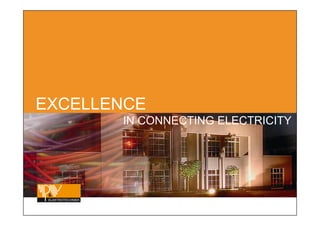
- 1. EXCELLENCE IN CONNECTING ELECTRICITY
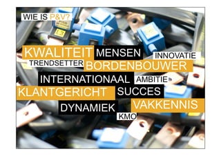
- 2. WIE IS P&V? KWALITEIT MENSEN INNOVATIE TRENDSETTER BORDENBOUWER INTERNATIONAAL AMBITIE KLANTGERICHT SUCCES DYNAMIEK VAKKENNIS KMO
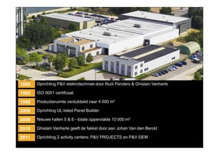
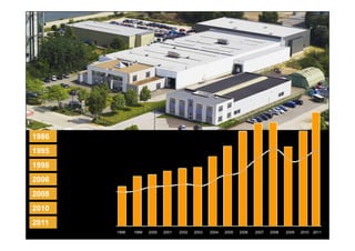
- 3. 1986 Oprichting P&V elektrotechniek door Rudi Penders & Ghislain Vanherle 1995 ISO 9001 certificaat 1998 Productieruimte verdubbeld naar 4 000 m? 2006 Oprichting UL listed Panel Builder 2008 Nieuwe hallen 5 & 6 - totale oppervlakte 10 000 m? 2010 Ghislain Vanherle geeft de fakkel door aan Johan Van den Berckt 2011 Oprichting 2 activity centers: P&V PROJECTS en P&V OEM
- 4. 1986 1995 1998 2006 2008 2010 2011 1998 1999 2000 2001 2002 2003 2004 2005 2006 2007 2008 2009 2010 2011
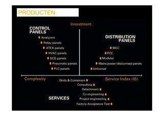
- 5. PRODUCTEN.
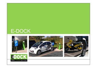
- 7. E-DOCK
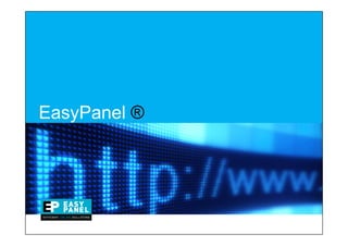
- 8. EasyPanel ? Atlas Copco
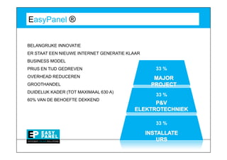
- 9. EasyPanel ? BELANGRIJKE INNOVATIE ER STAAT EEN NIEUWE INTERNET GENERATIE KLAAR BUSINESS MODEL PRIJS EN TIJD GEDREVEN 33 % OVERHEAD REDUCEREN MAJOR GROOTHANDEL PROJECT DUIDELIJK KADER (TOT MAXIMAAL 630 A) 33 % 60% VAN DE BEHOEFTE DEKKEND P&V ELEKTROTECHNIEK 33 % INSTALLATE URS
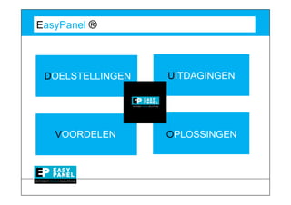
- 10. EasyPanel ? DOELSTELLINGEN UITDAGINGEN VOORDELEN OPLOSSINGEN
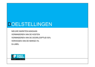
- 11. DOELSTELLINGEN NIEUWE MARKTEN AANGAAN VERMINDEREN VAN DE KOSTEN VERMINDEREN VAN DE DOORLOOPTIJD 50% VERHOGEN VAN DE MARGE 5% Q-LABEL
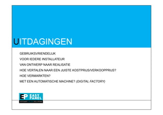
- 12. UITDAGINGEN GEBRUIKSVRIENDELIJK VOOR IEDERE INSTALLATEUR VAN ONTWERP NAAR REALISATIE HOE VERTALEN NAAR EEN JUISTE KOSTPRIJS/VERKOOPPRIJS? HOE VERMARKTEN? MET EEN AUTOMATISCHE MACHINE? (DIGITAL FACTORY)
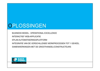
- 13. OPLOSSINGEN BUSINESS MODEL : OPERATIONAL EXCELLENCE INTERACTIEF WEB-APPLICATIE EPLAN AUTOMATISERINGSPLATFORM INTEGRATIE VAN DE VERSCHILLENDE WERKPROCESSEN TOT 1 GEHEEL SAMENWERKINGEN MET DE GROOTHANDEL/CONSTRUCTEURS
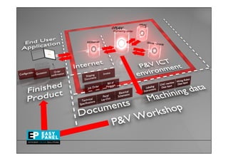
- 15. MOVIE
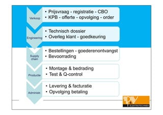
- 16. ? Prijsvraag - registratie - CBO Verkoop ? KPB - offerte - opvolging - order ? Technisch dossier Engineering ? Overleg klant - goedkeuring ? Bestellingen - goederenontvangst Supply chain ? Bevoorrading ? Montage & bedrading Productie ? Test & Q-control ? Levering & facturatie Administr. ? Opvolging betaling
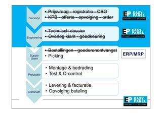
- 17. ? Prijsvraag - registratie - CBO Verkoop ? KPB - offerte - opvolging - order ? Technisch dossier Engineering ? Overleg klant - goedkeuring ? Bestellingen - goederenontvangst Supply ? Picking ERP/MRP chain ? Montage & bedrading Productie ? Test & Q-control ? Levering & facturatie Administr. ? Opvolging betaling
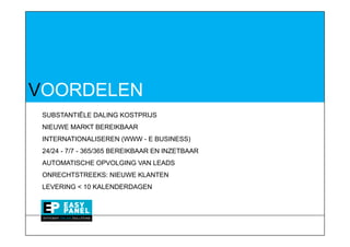
- 18. VOORDELEN SUBSTANTI?LE DALING KOSTPRIJS NIEUWE MARKT BEREIKBAAR INTERNATIONALISEREN (WWW - E BUSINESS) 24/24 - 7/7 - 365/365 BEREIKBAAR EN INZETBAAR AUTOMATISCHE OPVOLGING VAN LEADS ONRECHTSTREEKS: NIEUWE KLANTEN LEVERING < 10 KALENDERDAGEN
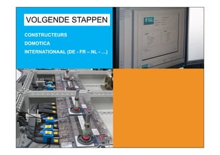
- 19. VOLGENDE STAPPEN CONSTRUCTEURS DOMOTICA INTERNATIONAAL (DE - FR ¨C NL - ¡)
- 20. Q&A