際際滷

際際滷Share a Scribd company logo
PCB Tutorial
Steps in Designing a PCB
? DECIDE WHAT FUNCTIONALITY YOU NEED
? Break that functionality into small modules
? Sense motion -> IMU
? Communicate with phone -> Bluetooth module
? Research components for each module
? Always read the datasheets
? Check to make sure footprints are solderable
? Choose a CPU that can interface with your modules and meets other requirements
? Try not to pick something overly complicated
Steps in Designing a PCB
? MAKE THE SYSTEM SCHEMATIC
? Confirm every part has a schematic symbol and footprint
? If it doesn¨t then make your own
? Place all parts on the schematic and wire
? Remember to add lots of bypass caps
? Check errors to make sure everything is properly connected
? MAKE PCB
? Check design rules
? Place parts in reasonable location (minimize rats nest)
? Use polygon pours for power and ground
? Route remaining traces (use larger width for high current)
? Check DRC
Interacting with Schematic Parts
? ALL PARTS HAVE A CROSSHAIR THAT CAN BE INTERACTED WITH
? KIND OF GOOFY FOR SOME PARTS LIKE FRAME
? WHEN SELECTING MULTIPLE OBJECTS, SOME COMMANDS LIKE MOVE REQUIRE RIGHT
CLICKING TO AFFECT THE WHOLE GROUP
Wiring it Up
? USE NET TOOL TO MAKE CONNECTIONS
? DON¨T ALWAYS NEED TO MAKE A PHYSICAL CONNECTION
? Create a partial net
? Use the name tool to give it a proper name
? Use the label tool to place that name right on the net
? Repeat for other pins you want to connect
? ALWAYS DO AN ERC WHEN FINISHED TO FIND ANY MISTAKES.
PCB Layout
? USE FILE -> SWITCH TO SCHEMATIC TO CREATE A PCB FOR YOUR SCHEMATIC
? FIRST SET UP YOUR GRID, USUALLY WANT A SLIGHTLY LARGE GRID AND A MUCH
SMALLER ALT GRID
? NEXT, USE DRC TO SET UP DESIGN RULES ACCORDING TO PCB MANUFACTURER
REQUIREMENTS
? Can download and import Osh Park DRU
? WHEN MOVING PARTS, EVERYTHING SNAPS TO GRID, CAN HOLD ALT KEY TO GET MORE
FINE GRAINED CONTROL
? TRY TO ARRANGE PARTS TO MINIMIZE THE RAT¨S NEST
Altium Layers
Routing
? CURRENT OPERATING LAYER SHOWN IN UPPER LEFT
? CLICK MIDDLE MOUSE BUTTON TO SWITCH
? FOCUS ON ONE TRACE AT A TIME
? Use middle click to place a via
? Right click to change wire style
? For tight boards, try to keep top layer horizontal and bottom layer vertical
? Use bigger traces for power and ground if possible
? WHEN FINISHED, USE RATS NEST TO CHECK IF ANYTHING MISSED
? ALWAYS DO A DRC
Advanced Routing
? GOOD IDEA TO USE POLYGON POURS FOR POWER AND GROUND
? Provides good capacitance to reduce noise
? Makes routing easier
? Looks cool
? USE POLYGON POUR TOOL TO TRACE OUTLINE
? PRESS RATSNEST TO FILL IN.
? CAN STILL ROUTE THROUGH THE POUR OR HIDE WITH RIPUP ON THE EDGE
? ALSO FUN TO WRITE ON THE BOARD BY EDITING THE SILKSCREEN
? Choose tPlace or bPlace layer then use drawing or text tools
? Wont affect circuit, purely visual
Finishing Up
? NEED TO CONVERT SCHEMATIC TO FORMAT A PCB MANUFACTURER CAN PARSE
? Standard to use Gerber files
? Need one Gerber file for each layer of the board
? PRESS THE CAM TOOL BUTTON
? Open job, choose the sparkfun job file
? Process job
? Zip the cam files up and submit to Osh Park
Creating Custom Parts
? FROM THE CONTROL PANEL GO TO FILE -> NEW -> LIBRARY
? LIBRARY -> SYMBOL, NAME IT AND ACCEPT
? THIS OPENS AN EDITOR SIMILAR TO A SCHEMATIC
? Use shapes to draw a box
? Use the add pins tool to place pins on the box
? Name the pins
? Good idea to add >NAME and >VALUE text to part to allow more customization down the line,
make sure to set these to Names and Values layer respectively
? Save and then go to Library -> Create -> Package
Creating Custom Footprints
? START BY USING THE SMD OR PAD TOOL TO PLACE PADS
? CAN CHANGE TO METRIC UNITS USING GRID
? SET SIZE OF PADS WITH INFO TOOL
? THE GRID IS YOUR FRIEND
? Set the grid distance to be the distance between pads for quick and easy placement
? Hold control while moving to have pads center on grid
? Can also use info to explicitly choose center
? USE TPLACE LAYER TO DRAW SHAPE OF CHIP BODY (OPTIONAL)
? ADD >NAME AND >VALUE TEXT IN TNAME AND TVALUE LAYERS
Associate Symbol and Package
? LIBRARY -> DEVICE -> NEW
? Name it the same thing as the Symbol and Package
? USE ADD TO PLACE THE SYMBOL FOR THE PART
? IN THE RIGHT SIDE, PRESS NEW AND ADD THE PACKAGE
? Note the yellow exclamation, this means pins have not been associated
? DOUBLE CLICK ON THE PACKAGE NAME TO ASSOCIATE
? SET PREFIX (DEFAULT IS U)
? MATCH LEFT AND RIGHT SIDES THEN PRESS CONNECT
? SAVE AND YOU¨RE DONE!
? FIND YOUR LIBRARY IN THE CONTROL PANEL, RIGHT CLICK AND USE
Thank You

More Related Content

Similar to PCB Tutorial.pptx (20)

PPTX
TA ESE 555
sushilpanda
?
PPTX
introductions to Stata software power point
MuzayenSheko1
?
PPTX
ORCAD pcb design
JHALAKNIHALANI
?
PPTX
FLOWCHART Discussion and Activities.pptx
Chin Chanie
?
PDF
Creating Living Style Guides to Improve Performance
Nicole Sullivan
?
DOCX
Computing fundamentals lab record - Polytechnics
SHAMJITH KM
?
DOCX
PCB Artist Desinging Software Report
Er. Ashish Pandey
?
PDF
Going responsive
Robert Cochran
?
PDF
pm1
Phil Mason
?
PDF
Revit shortcuts keyboard shortcuts & commands autodesk
pinoy cadplus
?
PPTX
Flow Chajhbhvhhhhhhhhhhhhhrts FOR BPE.pptx
develvin404
?
PDF
Six_Sigma_Spurious_12_15_09
Dr. Ali Nassib
?
PPT
Stack It And Unpack It
Jeff Moss
?
PPT
Project_PPT_Presentation.ppt
BIPLABNAYAK10
?
PPTX
3 D Printing Tutorial
Matthew Andrews
?
PPTX
Flowchart
archiesalangsang
?
PDF
Power hour 9 | Trello - Stay focused and organise your day
TheoRuby
?
PPTX
Dip trace tutorial
Mahadev Gopalakrishnan
?
TA ESE 555
sushilpanda
?
introductions to Stata software power point
MuzayenSheko1
?
ORCAD pcb design
JHALAKNIHALANI
?
FLOWCHART Discussion and Activities.pptx
Chin Chanie
?
Creating Living Style Guides to Improve Performance
Nicole Sullivan
?
Computing fundamentals lab record - Polytechnics
SHAMJITH KM
?
PCB Artist Desinging Software Report
Er. Ashish Pandey
?
Going responsive
Robert Cochran
?
Revit shortcuts keyboard shortcuts & commands autodesk
pinoy cadplus
?
Flow Chajhbhvhhhhhhhhhhhhhrts FOR BPE.pptx
develvin404
?
Six_Sigma_Spurious_12_15_09
Dr. Ali Nassib
?
Stack It And Unpack It
Jeff Moss
?
Project_PPT_Presentation.ppt
BIPLABNAYAK10
?
3 D Printing Tutorial
Matthew Andrews
?
Power hour 9 | Trello - Stay focused and organise your day
TheoRuby
?
Dip trace tutorial
Mahadev Gopalakrishnan
?

More from Godwin585235 (10)

PPTX
Arduino-Workshop For beginners UG Students
Godwin585235
?
PPTX
Tech rat ppt for the engineering students.pptx
Godwin585235
?
PPTX
VEHICLE TO VEHICLE COMMUNICATION USING LI-FI TECHNOLOGY (2).pptx
Godwin585235
?
PPT
notwa dfdfvs gf fdgfgh s thgfgh frg reggg
Godwin585235
?
PPTX
digita circuit design.pptx
Godwin585235
?
PPT
java01.ppt
Godwin585235
?
PPT
ch02.ppt
Godwin585235
?
PPTX
cyber secuirty.pptx
Godwin585235
?
PPTX
ROBOTICS APPLICATIONS.pptx
Godwin585235
?
PPTX
Presentation On Machine Learning.pptx
Godwin585235
?
Arduino-Workshop For beginners UG Students
Godwin585235
?
Tech rat ppt for the engineering students.pptx
Godwin585235
?
VEHICLE TO VEHICLE COMMUNICATION USING LI-FI TECHNOLOGY (2).pptx
Godwin585235
?
notwa dfdfvs gf fdgfgh s thgfgh frg reggg
Godwin585235
?
digita circuit design.pptx
Godwin585235
?
java01.ppt
Godwin585235
?
ch02.ppt
Godwin585235
?
cyber secuirty.pptx
Godwin585235
?
ROBOTICS APPLICATIONS.pptx
Godwin585235
?
Presentation On Machine Learning.pptx
Godwin585235
?
Ad

Recently uploaded (20)

PDF
Module - 5 Machine Learning-22ISE62.pdf
Dr. Shivashankar
?
PDF
Artificial Neural Network-Types,Perceptron,Problems
Sharmila Chidaravalli
?
PDF
PROGRAMMING REQUESTS/RESPONSES WITH GREATFREE IN THE CLOUD ENVIRONMENT
samueljackson3773
?
PPTX
Electrical_Safety_EMI_EMC_Presentation.pptx
drmaneharshalid
?
PPSX
OOPS Concepts in Python and Exception Handling
Dr. A. B. Shinde
?
PPTX
Precooling and Refrigerated storage.pptx
ThongamSunita
?
PDF
William Stallings - Foundations of Modern Networking_ SDN, NFV, QoE, IoT, and...
lavanya896395
?
DOCX
Engineering Geology Field Report to Malekhu .docx
justprashant567
?
PPTX
Kel.3_A_Review_on_Internet_of_Things_for_Defense_v3.pptx
Endang Saefullah
?
PDF
Plant Control_EST_85520-01_en_AllChanges_20220127.pdf
DarshanaChathuranga4
?
PDF
NFPA 10 - Estandar para extintores de incendios portatiles (ed.22 ENG).pdf
Oscar Orozco
?
PPTX
CM Function of the heart pp.pptxafsasdfddsf
drmaneharshalid
?
PPTX
UNIT 1 - INTRODUCTION TO AI and AI tools and basic concept
gokuld13012005
?
PDF
bs-en-12390-3 testing hardened concrete.pdf
ADVANCEDCONSTRUCTION
?
PDF
Bayesian Learning - Naive Bayes Algorithm
Sharmila Chidaravalli
?
PPTX
Stability of IBR Dominated Grids - IEEE PEDG 2025 - short.pptx
ssuser307730
?
PPTX
FSE_LLM4SE1_A Tool for In-depth Analysis of Code Execution Reasoning of Large...
cl144
?
PDF
13th International Conference on Artificial Intelligence, Soft Computing (AIS...
ijait
?
PPTX
Explore USA¨s Best Structural And Non Structural Steel Detailing
Silicon Engineering Consultants LLC
?
PDF
i氏Y創_Miipher and Miipher2 .
鰻粥京晦粥皆幄塀氏芙
?
Module - 5 Machine Learning-22ISE62.pdf
Dr. Shivashankar
?
Artificial Neural Network-Types,Perceptron,Problems
Sharmila Chidaravalli
?
PROGRAMMING REQUESTS/RESPONSES WITH GREATFREE IN THE CLOUD ENVIRONMENT
samueljackson3773
?
Electrical_Safety_EMI_EMC_Presentation.pptx
drmaneharshalid
?
OOPS Concepts in Python and Exception Handling
Dr. A. B. Shinde
?
Precooling and Refrigerated storage.pptx
ThongamSunita
?
William Stallings - Foundations of Modern Networking_ SDN, NFV, QoE, IoT, and...
lavanya896395
?
Engineering Geology Field Report to Malekhu .docx
justprashant567
?
Kel.3_A_Review_on_Internet_of_Things_for_Defense_v3.pptx
Endang Saefullah
?
Plant Control_EST_85520-01_en_AllChanges_20220127.pdf
DarshanaChathuranga4
?
NFPA 10 - Estandar para extintores de incendios portatiles (ed.22 ENG).pdf
Oscar Orozco
?
CM Function of the heart pp.pptxafsasdfddsf
drmaneharshalid
?
UNIT 1 - INTRODUCTION TO AI and AI tools and basic concept
gokuld13012005
?
bs-en-12390-3 testing hardened concrete.pdf
ADVANCEDCONSTRUCTION
?
Bayesian Learning - Naive Bayes Algorithm
Sharmila Chidaravalli
?
Stability of IBR Dominated Grids - IEEE PEDG 2025 - short.pptx
ssuser307730
?
FSE_LLM4SE1_A Tool for In-depth Analysis of Code Execution Reasoning of Large...
cl144
?
13th International Conference on Artificial Intelligence, Soft Computing (AIS...
ijait
?
Explore USA¨s Best Structural And Non Structural Steel Detailing
Silicon Engineering Consultants LLC
?
i氏Y創_Miipher and Miipher2 .
鰻粥京晦粥皆幄塀氏芙
?
Ad

PCB Tutorial.pptx

  • 2. Steps in Designing a PCB ? DECIDE WHAT FUNCTIONALITY YOU NEED ? Break that functionality into small modules ? Sense motion -> IMU ? Communicate with phone -> Bluetooth module ? Research components for each module ? Always read the datasheets ? Check to make sure footprints are solderable ? Choose a CPU that can interface with your modules and meets other requirements ? Try not to pick something overly complicated
  • 3. Steps in Designing a PCB ? MAKE THE SYSTEM SCHEMATIC ? Confirm every part has a schematic symbol and footprint ? If it doesn¨t then make your own ? Place all parts on the schematic and wire ? Remember to add lots of bypass caps ? Check errors to make sure everything is properly connected ? MAKE PCB ? Check design rules ? Place parts in reasonable location (minimize rats nest) ? Use polygon pours for power and ground ? Route remaining traces (use larger width for high current) ? Check DRC
  • 4. Interacting with Schematic Parts ? ALL PARTS HAVE A CROSSHAIR THAT CAN BE INTERACTED WITH ? KIND OF GOOFY FOR SOME PARTS LIKE FRAME ? WHEN SELECTING MULTIPLE OBJECTS, SOME COMMANDS LIKE MOVE REQUIRE RIGHT CLICKING TO AFFECT THE WHOLE GROUP
  • 5. Wiring it Up ? USE NET TOOL TO MAKE CONNECTIONS ? DON¨T ALWAYS NEED TO MAKE A PHYSICAL CONNECTION ? Create a partial net ? Use the name tool to give it a proper name ? Use the label tool to place that name right on the net ? Repeat for other pins you want to connect ? ALWAYS DO AN ERC WHEN FINISHED TO FIND ANY MISTAKES.
  • 6. PCB Layout ? USE FILE -> SWITCH TO SCHEMATIC TO CREATE A PCB FOR YOUR SCHEMATIC ? FIRST SET UP YOUR GRID, USUALLY WANT A SLIGHTLY LARGE GRID AND A MUCH SMALLER ALT GRID ? NEXT, USE DRC TO SET UP DESIGN RULES ACCORDING TO PCB MANUFACTURER REQUIREMENTS ? Can download and import Osh Park DRU ? WHEN MOVING PARTS, EVERYTHING SNAPS TO GRID, CAN HOLD ALT KEY TO GET MORE FINE GRAINED CONTROL ? TRY TO ARRANGE PARTS TO MINIMIZE THE RAT¨S NEST
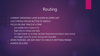
  • 8. Routing ? CURRENT OPERATING LAYER SHOWN IN UPPER LEFT ? CLICK MIDDLE MOUSE BUTTON TO SWITCH ? FOCUS ON ONE TRACE AT A TIME ? Use middle click to place a via ? Right click to change wire style ? For tight boards, try to keep top layer horizontal and bottom layer vertical ? Use bigger traces for power and ground if possible ? WHEN FINISHED, USE RATS NEST TO CHECK IF ANYTHING MISSED ? ALWAYS DO A DRC
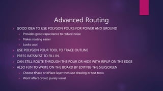
  • 9. Advanced Routing ? GOOD IDEA TO USE POLYGON POURS FOR POWER AND GROUND ? Provides good capacitance to reduce noise ? Makes routing easier ? Looks cool ? USE POLYGON POUR TOOL TO TRACE OUTLINE ? PRESS RATSNEST TO FILL IN. ? CAN STILL ROUTE THROUGH THE POUR OR HIDE WITH RIPUP ON THE EDGE ? ALSO FUN TO WRITE ON THE BOARD BY EDITING THE SILKSCREEN ? Choose tPlace or bPlace layer then use drawing or text tools ? Wont affect circuit, purely visual
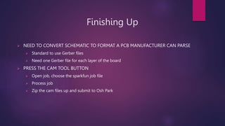
  • 10. Finishing Up ? NEED TO CONVERT SCHEMATIC TO FORMAT A PCB MANUFACTURER CAN PARSE ? Standard to use Gerber files ? Need one Gerber file for each layer of the board ? PRESS THE CAM TOOL BUTTON ? Open job, choose the sparkfun job file ? Process job ? Zip the cam files up and submit to Osh Park
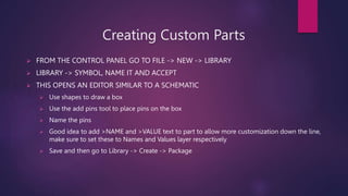
  • 11. Creating Custom Parts ? FROM THE CONTROL PANEL GO TO FILE -> NEW -> LIBRARY ? LIBRARY -> SYMBOL, NAME IT AND ACCEPT ? THIS OPENS AN EDITOR SIMILAR TO A SCHEMATIC ? Use shapes to draw a box ? Use the add pins tool to place pins on the box ? Name the pins ? Good idea to add >NAME and >VALUE text to part to allow more customization down the line, make sure to set these to Names and Values layer respectively ? Save and then go to Library -> Create -> Package
  • 12. Creating Custom Footprints ? START BY USING THE SMD OR PAD TOOL TO PLACE PADS ? CAN CHANGE TO METRIC UNITS USING GRID ? SET SIZE OF PADS WITH INFO TOOL ? THE GRID IS YOUR FRIEND ? Set the grid distance to be the distance between pads for quick and easy placement ? Hold control while moving to have pads center on grid ? Can also use info to explicitly choose center ? USE TPLACE LAYER TO DRAW SHAPE OF CHIP BODY (OPTIONAL) ? ADD >NAME AND >VALUE TEXT IN TNAME AND TVALUE LAYERS
  • 13. Associate Symbol and Package ? LIBRARY -> DEVICE -> NEW ? Name it the same thing as the Symbol and Package ? USE ADD TO PLACE THE SYMBOL FOR THE PART ? IN THE RIGHT SIDE, PRESS NEW AND ADD THE PACKAGE ? Note the yellow exclamation, this means pins have not been associated ? DOUBLE CLICK ON THE PACKAGE NAME TO ASSOCIATE ? SET PREFIX (DEFAULT IS U) ? MATCH LEFT AND RIGHT SIDES THEN PRESS CONNECT ? SAVE AND YOU¨RE DONE! ? FIND YOUR LIBRARY IN THE CONTROL PANEL, RIGHT CLICK AND USE