ºÝºÝߣ

ºÝºÝߣShare a Scribd company logo
TIMING ANALYSIS OF  LOGIC CIRCUITS
Post layout simulation HDL Implementation Design Cycle DESIGN ENTRY Schematic , VHDL, Verilog, etc. Functional Simulation SYNTHESIS Test insertion Gate level simulation Implementation MAP, PLACE , ROUTE Static Timing Analysis Static Timing Analysis Libraries Constraints
The Timing Analyzer performs a static timing analysis of a mapped design A static timing analysis is a point-to-point analysis of a design network. The Timing Analyzer verifies that the delay along a given path or paths meets your specified timing requirements. It organizes and displays data that allows you to analyze the critical paths in your circuit, the cycle time of the circuit, the delay along any specified paths. Timing Analysis of Logic Circuits
Static timing analysis is performed at various stages of the design flow viz. after synthesis, after test insertion, after layout, etc. Your design's system performance is limited by some basic types of timing paths. Each of these paths goes through a sequence of logic, routing, and logic. Timing Analysis of Logic Circuits
Why Static Timing Analysis ? Verifying the timings of designs with millions of gates using dynamic timing analysis may prove to be impossible due to very high run times.  Dynamic simulation relies on the quality and coverage of the test bench.  Static timing analysis is very very fast as compared to dynamic analysis and verifies all parts of the gate level design. Static timing analysis does not check the functionality of the design. Extensive dynamic simulation is required to verify the functionality.
Pad to Pad A pad-to-pad path starts at an input pad of the chip, propagates through one or more levels of combinational logic, and ends at an output pad of the chip. The pad-to-pad path time is the maximum time required for the data to enter the chip, travel through logic & routing, and leave the chip.  It is not controlled or affected by any clock signal.
Pad To Pad
Pad to Setup  A pad-to-setup path starts at an input pad of the chip, propagates through input buffers and any number of combinatorial logic levels, and end at a D/T input to a flip-flop, latch or the receiving flip-flop’s t setup. Pad-to-set paths do not travel through flip-flops. The pad-to-setup path time is the maximum time required for the data to enter the chip, travel through logic and routing, and arrive at the input (D/T) before the clock or control signal arrives.
Pad To Setup
Clock To Pad Paths  A clock-to-pad path starts at a clock input of a flip-flop, propagates through the flip-flop Q output and any number of levels of  combinatorial logic, and ends at an output pad.  It includes the clock-to-Q delay (Tpff) of the flip-flop and the path delay from that flip-flop to the chip output. The clock-to-pad path time is the maximum time required for the data to leave the source flip-flop, travel through logic & routing, and leave the chip.
Clock To Pad Paths
Clock To Pad Through Tristates
These are not valid clock to pad paths.
Clock To Setup - Same Clock
Rising Edge To Falling Edge Timing
Falling Edge To Rising Edge
Clock To Setup - Different Clocks
The paths ending at the clock pin of other FFs or the asynchronous pins of other FFs are not valid clock to setup paths. Clock enable pins ? They are similar to data. They will also have setup requirement.
Clock Pad To Clock Pin Of F/Fs
E.g. 1 What is the minimum clock period (Tmin) for this circuit? Hint: Evaluate all FF to FF paths
E.g. 1 contd. Path FFA to FFB TClk-Q(FFA) + Tpd(H) + Ts(FFB) =  5ns + 5ns+ 2ns = 12ns Path FFB to FFB TCLK-Q(FFB) + Tpd(F) + Tpd(H) + Ts(FFB) =  4ns + 4ns + 5ns + 2n = 15 ns   So, Tmin=15 ns.
E.g. 2 Analysis of All The Paths In The Circuit
E.g. 2 Analysis of All The Paths In The Circuit Data at A, B, C and D is stable for 3 ns after the rising clock edge Data at X and Y has to be stable 3 ns before the rising clock edge. Calculate the maximum frequency of operation of the circuit. The delays are  Tpd AND,OR= 1 ns, Tpd XOR= 2 ns, Tsetup= 1 ns, TclocktoQ  = 3 ns.
E.g. 2 contd. Pad to Pad A to Y: (i) Tin-G4-Tout = 3+1+3=7ns (ii) Tin-G1-G4-Tout = 3+1+1+3=8ns
Pad to clock A-FF2D (i) Tin-G4-G7-TsetupFF2 =3+1+2+1=7ns (ii) Tin-G1-G4-G7-TsetupFF2 =3+1+1+2+1=8ns (iii) Tin-G5-G6-G7-TsetupFF2    =3+1+1+1+2+1=9ns C-FF2D: Tin-G3-G7-TsetupFF2 =3+1+2+1=7ns D-FF2D: Tin-G2-G5-G6-G7-TsetupFF2    =3+1+1+1+2+1=9ns C-FF2E Tin-G8-TsetupFF2 = 3+1+1=5ns D-FF2E Tin-G2-G5-G6-G8-TsetupFF2 =3+1+1+1+1+1=8ns
Clock to clock path FF1D – FF2D:  (i)Tclk-QFF1-G1-G4-G7-TsetupFF2 = 3+1+1+2+1 = 8ns (ii) Tclk-QFF1-G1-G5-G6-G7-TsetupFF2 = 3+1+1+1+2+1 = 9ns (iii) Tclk-QFF1-G2-G5-G6-G7-TsetupFF2 = 3+1+1+1+2+1 = 9ns (iv)Tclk-QnFF1-G6-G7-TsetupFF2 = 3+1+2+1 = 7ns (iv)Tclk-QnFF1-G3-G7-TsetupFF2 = 3+1+2+1 = 7ns
Clock to clock path (contd.) FF1D – FF2E:  (i) Tclk-QFF1-G1-G5-G6-G8-TsetupFF2 = 3+1+1+1+1+1 = 8ns (ii) Tclk-QFF1-G2-G5-G6-G8-TsetupFF2 = 3+1+1+1+1+1 = 8ns (iii)Tclk-QnFF1-G6-G8-TsetupFF2 = 3+1+1+1 = 6ns
Clock to Pad  FF1 – Y:  (i) Tclk-QFF1-G1-G4-Tout = 3+1+1+3 = 8ns FF2 – X (i) Tclk-QFF2-Tout = 3+3 = 6ns Maximum period between clk to clk paths is 9 ns Maximum frequency of operation = 1/9  =111.11 Mhz
THANK YOU

More Related Content

What's hot (20)

Timing and Design Closure in Physical Design Flows
Timing and Design Closure in Physical Design Flows Timing and Design Closure in Physical Design Flows
Timing and Design Closure in Physical Design Flows
Olivier Coudert
Ìý
Floor plan & Power Plan
Floor plan & Power Plan Floor plan & Power Plan
Floor plan & Power Plan
Prathyusha Madapalli
Ìý
VLSI-Physical Design- Tool Terminalogy
VLSI-Physical Design- Tool TerminalogyVLSI-Physical Design- Tool Terminalogy
VLSI-Physical Design- Tool Terminalogy
Murali Rai
Ìý
Timing analysis
Timing analysisTiming analysis
Timing analysis
Kunal Doshi
Ìý
Define Width and Height of Core and Die (http://www.vlsisystemdesign.com/PD-F...
Define Width and Height of Core and Die (http://www.vlsisystemdesign.com/PD-F...Define Width and Height of Core and Die (http://www.vlsisystemdesign.com/PD-F...
Define Width and Height of Core and Die (http://www.vlsisystemdesign.com/PD-F...
VLSI SYSTEM Design
Ìý
12 static timing_analysis_3_clocked_design
12 static timing_analysis_3_clocked_design12 static timing_analysis_3_clocked_design
12 static timing_analysis_3_clocked_design
Usha Mehta
Ìý
GUI for DRV fix in ICC2
GUI for DRV fix in ICC2GUI for DRV fix in ICC2
GUI for DRV fix in ICC2
Prashanth Chokkarapu
Ìý
Inputs of physical design
Inputs of physical designInputs of physical design
Inputs of physical design
Kishore Sai Addanki
Ìý
13 static timing_analysis_4_set_up_and_hold_time_violation_remedy
13 static timing_analysis_4_set_up_and_hold_time_violation_remedy13 static timing_analysis_4_set_up_and_hold_time_violation_remedy
13 static timing_analysis_4_set_up_and_hold_time_violation_remedy
Usha Mehta
Ìý
Understanding cts log_messages
Understanding cts log_messagesUnderstanding cts log_messages
Understanding cts log_messages
Mujahid Mohammed
Ìý
Eco
EcoEco
Eco
Rajesh M
Ìý
Powerplanning
PowerplanningPowerplanning
Powerplanning
VLSI SYSTEM Design
Ìý
Physical Design Flow Challenges at 28nm on Multi-million Gate Blocks
Physical Design Flow Challenges at 28nm on Multi-million Gate BlocksPhysical Design Flow Challenges at 28nm on Multi-million Gate Blocks
Physical Design Flow Challenges at 28nm on Multi-million Gate Blocks
eInfochips (An Arrow Company)
Ìý
Multi mode multi corner (mmmc)
Multi mode multi corner (mmmc)Multi mode multi corner (mmmc)
Multi mode multi corner (mmmc)
shaik sharief
Ìý
Synopsys Fusion Compiler-Comprehensive RTL-to-GDSII Implementation System
Synopsys Fusion Compiler-Comprehensive RTL-to-GDSII Implementation SystemSynopsys Fusion Compiler-Comprehensive RTL-to-GDSII Implementation System
Synopsys Fusion Compiler-Comprehensive RTL-to-GDSII Implementation System
Mostafa Khamis
Ìý
Dft (design for testability)
Dft (design for testability)Dft (design for testability)
Dft (design for testability)
shaik sharief
Ìý
Digital VLSI Design : Introduction
Digital VLSI Design : IntroductionDigital VLSI Design : Introduction
Digital VLSI Design : Introduction
Usha Mehta
Ìý
Chapter1.slides
Chapter1.slidesChapter1.slides
Chapter1.slides
Avinash Pillai
Ìý
Complete ASIC design flow - VLSI UNIVERSE
Complete ASIC design flow - VLSI UNIVERSEComplete ASIC design flow - VLSI UNIVERSE
Complete ASIC design flow - VLSI UNIVERSE
VLSIUNIVERSE
Ìý
Vlsi physical design (Back End Process)
Vlsi physical design (Back End Process)Vlsi physical design (Back End Process)
Vlsi physical design (Back End Process)
CHENCHU CHANDU PRASANTH NADELLA
Ìý
Timing and Design Closure in Physical Design Flows
Timing and Design Closure in Physical Design Flows Timing and Design Closure in Physical Design Flows
Timing and Design Closure in Physical Design Flows
Olivier Coudert
Ìý
VLSI-Physical Design- Tool Terminalogy
VLSI-Physical Design- Tool TerminalogyVLSI-Physical Design- Tool Terminalogy
VLSI-Physical Design- Tool Terminalogy
Murali Rai
Ìý
Timing analysis
Timing analysisTiming analysis
Timing analysis
Kunal Doshi
Ìý
Define Width and Height of Core and Die (http://www.vlsisystemdesign.com/PD-F...
Define Width and Height of Core and Die (http://www.vlsisystemdesign.com/PD-F...Define Width and Height of Core and Die (http://www.vlsisystemdesign.com/PD-F...
Define Width and Height of Core and Die (http://www.vlsisystemdesign.com/PD-F...
VLSI SYSTEM Design
Ìý
12 static timing_analysis_3_clocked_design
12 static timing_analysis_3_clocked_design12 static timing_analysis_3_clocked_design
12 static timing_analysis_3_clocked_design
Usha Mehta
Ìý
13 static timing_analysis_4_set_up_and_hold_time_violation_remedy
13 static timing_analysis_4_set_up_and_hold_time_violation_remedy13 static timing_analysis_4_set_up_and_hold_time_violation_remedy
13 static timing_analysis_4_set_up_and_hold_time_violation_remedy
Usha Mehta
Ìý
Understanding cts log_messages
Understanding cts log_messagesUnderstanding cts log_messages
Understanding cts log_messages
Mujahid Mohammed
Ìý
Physical Design Flow Challenges at 28nm on Multi-million Gate Blocks
Physical Design Flow Challenges at 28nm on Multi-million Gate BlocksPhysical Design Flow Challenges at 28nm on Multi-million Gate Blocks
Physical Design Flow Challenges at 28nm on Multi-million Gate Blocks
eInfochips (An Arrow Company)
Ìý
Multi mode multi corner (mmmc)
Multi mode multi corner (mmmc)Multi mode multi corner (mmmc)
Multi mode multi corner (mmmc)
shaik sharief
Ìý
Synopsys Fusion Compiler-Comprehensive RTL-to-GDSII Implementation System
Synopsys Fusion Compiler-Comprehensive RTL-to-GDSII Implementation SystemSynopsys Fusion Compiler-Comprehensive RTL-to-GDSII Implementation System
Synopsys Fusion Compiler-Comprehensive RTL-to-GDSII Implementation System
Mostafa Khamis
Ìý
Dft (design for testability)
Dft (design for testability)Dft (design for testability)
Dft (design for testability)
shaik sharief
Ìý
Digital VLSI Design : Introduction
Digital VLSI Design : IntroductionDigital VLSI Design : Introduction
Digital VLSI Design : Introduction
Usha Mehta
Ìý
Complete ASIC design flow - VLSI UNIVERSE
Complete ASIC design flow - VLSI UNIVERSEComplete ASIC design flow - VLSI UNIVERSE
Complete ASIC design flow - VLSI UNIVERSE
VLSIUNIVERSE
Ìý

Viewers also liked (20)

FIFOPt
FIFOPtFIFOPt
FIFOPt
sumeet jain
Ìý
Roman Korkikyan - Timing analysis workshop Part 1 Theory
Roman Korkikyan - Timing analysis workshop Part 1 TheoryRoman Korkikyan - Timing analysis workshop Part 1 Theory
Roman Korkikyan - Timing analysis workshop Part 1 Theory
DefconRussia
Ìý
Roman Korkikyan - Timing analysis workshop Part 2 Practice
Roman Korkikyan - Timing analysis workshop Part 2 PracticeRoman Korkikyan - Timing analysis workshop Part 2 Practice
Roman Korkikyan - Timing analysis workshop Part 2 Practice
DefconRussia
Ìý
SNUG 2011 paper
SNUG 2011 paperSNUG 2011 paper
SNUG 2011 paper
David Tester
Ìý
Aldec overview 2011-10 revised
Aldec overview 2011-10 revisedAldec overview 2011-10 revised
Aldec overview 2011-10 revised
Prateek Chopra
Ìý
System Verilog 2009 & 2012 enhancements
System Verilog 2009 & 2012 enhancementsSystem Verilog 2009 & 2012 enhancements
System Verilog 2009 & 2012 enhancements
Subash John
Ìý
Session 9 advance_verification_features
Session 9 advance_verification_featuresSession 9 advance_verification_features
Session 9 advance_verification_features
Nirav Desai
Ìý
System Verilog Functional Coverage
System Verilog Functional CoverageSystem Verilog Functional Coverage
System Verilog Functional Coverage
rraimi
Ìý
tau 2015 spyrou fpga timing
tau 2015 spyrou fpga timingtau 2015 spyrou fpga timing
tau 2015 spyrou fpga timing
Tom Spyrou
Ìý
System verilog important
System verilog importantSystem verilog important
System verilog important
elumalai7
Ìý
System Verilog Tutorial - VHDL
System Verilog Tutorial - VHDLSystem Verilog Tutorial - VHDL
System Verilog Tutorial - VHDL
E2MATRIX
Ìý
system verilog
system verilogsystem verilog
system verilog
Vinchipsytm Vlsitraining
Ìý
Fundamentals of HDL (first 4 chapters only) - Godse
Fundamentals of HDL (first 4 chapters only) - GodseFundamentals of HDL (first 4 chapters only) - Godse
Fundamentals of HDL (first 4 chapters only) - Godse
Hammam
Ìý
System verilog verification building blocks
System verilog verification building blocksSystem verilog verification building blocks
System verilog verification building blocks
Nirav Desai
Ìý
FIFO Design
FIFO DesignFIFO Design
FIFO Design
Arrow Devices
Ìý
Simulation PowerPoint
Simulation PowerPointSimulation PowerPoint
Simulation PowerPoint
Melissa Wilson
Ìý
Delays in verilog
Delays in verilogDelays in verilog
Delays in verilog
JITU MISTRY
Ìý
Verilog HDL
Verilog HDLVerilog HDL
Verilog HDL
Mantra VLSI
Ìý
Fifo first in first out powerpoint ppt slides.
Fifo first in first out powerpoint ppt slides.Fifo first in first out powerpoint ppt slides.
Fifo first in first out powerpoint ppt slides.
ºÝºÝߣTeam.net
Ìý
First In, First Out (FIFO); Last In, Last Out (LIFO)
First In, First Out (FIFO); Last In, Last Out (LIFO)First In, First Out (FIFO); Last In, Last Out (LIFO)
First In, First Out (FIFO); Last In, Last Out (LIFO)
UNowAcademics
Ìý
Roman Korkikyan - Timing analysis workshop Part 1 Theory
Roman Korkikyan - Timing analysis workshop Part 1 TheoryRoman Korkikyan - Timing analysis workshop Part 1 Theory
Roman Korkikyan - Timing analysis workshop Part 1 Theory
DefconRussia
Ìý
Roman Korkikyan - Timing analysis workshop Part 2 Practice
Roman Korkikyan - Timing analysis workshop Part 2 PracticeRoman Korkikyan - Timing analysis workshop Part 2 Practice
Roman Korkikyan - Timing analysis workshop Part 2 Practice
DefconRussia
Ìý
SNUG 2011 paper
SNUG 2011 paperSNUG 2011 paper
SNUG 2011 paper
David Tester
Ìý
Aldec overview 2011-10 revised
Aldec overview 2011-10 revisedAldec overview 2011-10 revised
Aldec overview 2011-10 revised
Prateek Chopra
Ìý
System Verilog 2009 & 2012 enhancements
System Verilog 2009 & 2012 enhancementsSystem Verilog 2009 & 2012 enhancements
System Verilog 2009 & 2012 enhancements
Subash John
Ìý
Session 9 advance_verification_features
Session 9 advance_verification_featuresSession 9 advance_verification_features
Session 9 advance_verification_features
Nirav Desai
Ìý
System Verilog Functional Coverage
System Verilog Functional CoverageSystem Verilog Functional Coverage
System Verilog Functional Coverage
rraimi
Ìý
tau 2015 spyrou fpga timing
tau 2015 spyrou fpga timingtau 2015 spyrou fpga timing
tau 2015 spyrou fpga timing
Tom Spyrou
Ìý
System verilog important
System verilog importantSystem verilog important
System verilog important
elumalai7
Ìý
System Verilog Tutorial - VHDL
System Verilog Tutorial - VHDLSystem Verilog Tutorial - VHDL
System Verilog Tutorial - VHDL
E2MATRIX
Ìý
Fundamentals of HDL (first 4 chapters only) - Godse
Fundamentals of HDL (first 4 chapters only) - GodseFundamentals of HDL (first 4 chapters only) - Godse
Fundamentals of HDL (first 4 chapters only) - Godse
Hammam
Ìý
System verilog verification building blocks
System verilog verification building blocksSystem verilog verification building blocks
System verilog verification building blocks
Nirav Desai
Ìý
Simulation PowerPoint
Simulation PowerPointSimulation PowerPoint
Simulation PowerPoint
Melissa Wilson
Ìý
Delays in verilog
Delays in verilogDelays in verilog
Delays in verilog
JITU MISTRY
Ìý
Verilog HDL
Verilog HDLVerilog HDL
Verilog HDL
Mantra VLSI
Ìý
Fifo first in first out powerpoint ppt slides.
Fifo first in first out powerpoint ppt slides.Fifo first in first out powerpoint ppt slides.
Fifo first in first out powerpoint ppt slides.
ºÝºÝߣTeam.net
Ìý
First In, First Out (FIFO); Last In, Last Out (LIFO)
First In, First Out (FIFO); Last In, Last Out (LIFO)First In, First Out (FIFO); Last In, Last Out (LIFO)
First In, First Out (FIFO); Last In, Last Out (LIFO)
UNowAcademics
Ìý

Similar to Timing Analysis (20)

file-3.ppt
file-3.pptfile-3.ppt
file-3.ppt
teja411944
Ìý
file-3.ppt
file-3.pptfile-3.ppt
file-3.ppt
teja411944
Ìý
Te442 lecture02-2016-14-4-2016-1
Te442 lecture02-2016-14-4-2016-1Te442 lecture02-2016-14-4-2016-1
Te442 lecture02-2016-14-4-2016-1
colman mboya
Ìý
design-compiler.pdf
design-compiler.pdfdesign-compiler.pdf
design-compiler.pdf
FrangoCamila
Ìý
Major project iii 3
Major project  iii  3Major project  iii  3
Major project iii 3
Gopal Prasad Bansal
Ìý
Class 4 Static Timing Analysis.pptxkkkkkk
Class 4 Static Timing Analysis.pptxkkkkkkClass 4 Static Timing Analysis.pptxkkkkkk
Class 4 Static Timing Analysis.pptxkkkkkk
Anuragsiwach1
Ìý
Class 4 Static Timing Analysis.pptxkkkkkk
Class 4 Static Timing Analysis.pptxkkkkkkClass 4 Static Timing Analysis.pptxkkkkkk
Class 4 Static Timing Analysis.pptxkkkkkk
Anuragsiwach1
Ìý
Timing notes 2006
Timing notes 2006Timing notes 2006
Timing notes 2006
pavan kumar
Ìý
Timing closure document
Timing closure documentTiming closure document
Timing closure document
Alan Tran
Ìý
sta slide ref.pdf
sta slide ref.pdfsta slide ref.pdf
sta slide ref.pdf
quandao25
Ìý
Lecture-5-STA.pdf
Lecture-5-STA.pdfLecture-5-STA.pdf
Lecture-5-STA.pdf
KarthikYogesh3
Ìý
VLSI Static Timing Analysis Setup And Hold Part 2
VLSI Static Timing Analysis Setup And Hold Part 2VLSI Static Timing Analysis Setup And Hold Part 2
VLSI Static Timing Analysis Setup And Hold Part 2
Amr Adel
Ìý
15757597 (1).ppt
15757597 (1).ppt15757597 (1).ppt
15757597 (1).ppt
RevathiMohan14
Ìý
Level sensitive scan design(LSSD) and Boundry scan(BS)
Level sensitive scan design(LSSD) and Boundry scan(BS)Level sensitive scan design(LSSD) and Boundry scan(BS)
Level sensitive scan design(LSSD) and Boundry scan(BS)
Praveen Kumar
Ìý
A Robust UART Architecture Based on Recursive Running Sum Filter for Better N...
A Robust UART Architecture Based on Recursive Running Sum Filter for Better N...A Robust UART Architecture Based on Recursive Running Sum Filter for Better N...
A Robust UART Architecture Based on Recursive Running Sum Filter for Better N...
Kevin Mathew
Ìý
Tugas komjar 7-yee
Tugas komjar 7-yeeTugas komjar 7-yee
Tugas komjar 7-yee
ramasatriaf
Ìý
IEEE1588-v2
IEEE1588-v2IEEE1588-v2
IEEE1588-v2
Guider Lee
Ìý
07_Digital timing_&_Pipelining.ppt
07_Digital timing_&_Pipelining.ppt07_Digital timing_&_Pipelining.ppt
07_Digital timing_&_Pipelining.ppt
BUCHUPALLIVIMALAREDD2
Ìý
Verilog HDL Verification
Verilog HDL VerificationVerilog HDL Verification
Verilog HDL Verification
dennis gookyi
Ìý
FPGA Timing Models with electric motor system
FPGA Timing Models with electric motor systemFPGA Timing Models with electric motor system
FPGA Timing Models with electric motor system
sathyapriyar2350669
Ìý
file-3.ppt
file-3.pptfile-3.ppt
file-3.ppt
teja411944
Ìý
file-3.ppt
file-3.pptfile-3.ppt
file-3.ppt
teja411944
Ìý
Te442 lecture02-2016-14-4-2016-1
Te442 lecture02-2016-14-4-2016-1Te442 lecture02-2016-14-4-2016-1
Te442 lecture02-2016-14-4-2016-1
colman mboya
Ìý
design-compiler.pdf
design-compiler.pdfdesign-compiler.pdf
design-compiler.pdf
FrangoCamila
Ìý
Class 4 Static Timing Analysis.pptxkkkkkk
Class 4 Static Timing Analysis.pptxkkkkkkClass 4 Static Timing Analysis.pptxkkkkkk
Class 4 Static Timing Analysis.pptxkkkkkk
Anuragsiwach1
Ìý
Class 4 Static Timing Analysis.pptxkkkkkk
Class 4 Static Timing Analysis.pptxkkkkkkClass 4 Static Timing Analysis.pptxkkkkkk
Class 4 Static Timing Analysis.pptxkkkkkk
Anuragsiwach1
Ìý
Timing notes 2006
Timing notes 2006Timing notes 2006
Timing notes 2006
pavan kumar
Ìý
Timing closure document
Timing closure documentTiming closure document
Timing closure document
Alan Tran
Ìý
sta slide ref.pdf
sta slide ref.pdfsta slide ref.pdf
sta slide ref.pdf
quandao25
Ìý
Lecture-5-STA.pdf
Lecture-5-STA.pdfLecture-5-STA.pdf
Lecture-5-STA.pdf
KarthikYogesh3
Ìý
VLSI Static Timing Analysis Setup And Hold Part 2
VLSI Static Timing Analysis Setup And Hold Part 2VLSI Static Timing Analysis Setup And Hold Part 2
VLSI Static Timing Analysis Setup And Hold Part 2
Amr Adel
Ìý
15757597 (1).ppt
15757597 (1).ppt15757597 (1).ppt
15757597 (1).ppt
RevathiMohan14
Ìý
Level sensitive scan design(LSSD) and Boundry scan(BS)
Level sensitive scan design(LSSD) and Boundry scan(BS)Level sensitive scan design(LSSD) and Boundry scan(BS)
Level sensitive scan design(LSSD) and Boundry scan(BS)
Praveen Kumar
Ìý
A Robust UART Architecture Based on Recursive Running Sum Filter for Better N...
A Robust UART Architecture Based on Recursive Running Sum Filter for Better N...A Robust UART Architecture Based on Recursive Running Sum Filter for Better N...
A Robust UART Architecture Based on Recursive Running Sum Filter for Better N...
Kevin Mathew
Ìý
Tugas komjar 7-yee
Tugas komjar 7-yeeTugas komjar 7-yee
Tugas komjar 7-yee
ramasatriaf
Ìý
IEEE1588-v2
IEEE1588-v2IEEE1588-v2
IEEE1588-v2
Guider Lee
Ìý
07_Digital timing_&_Pipelining.ppt
07_Digital timing_&_Pipelining.ppt07_Digital timing_&_Pipelining.ppt
07_Digital timing_&_Pipelining.ppt
BUCHUPALLIVIMALAREDD2
Ìý
Verilog HDL Verification
Verilog HDL VerificationVerilog HDL Verification
Verilog HDL Verification
dennis gookyi
Ìý
FPGA Timing Models with electric motor system
FPGA Timing Models with electric motor systemFPGA Timing Models with electric motor system
FPGA Timing Models with electric motor system
sathyapriyar2350669
Ìý

Timing Analysis

  • 1. TIMING ANALYSIS OF LOGIC CIRCUITS
  • 2. Post layout simulation HDL Implementation Design Cycle DESIGN ENTRY Schematic , VHDL, Verilog, etc. Functional Simulation SYNTHESIS Test insertion Gate level simulation Implementation MAP, PLACE , ROUTE Static Timing Analysis Static Timing Analysis Libraries Constraints
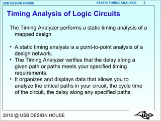
  • 3. The Timing Analyzer performs a static timing analysis of a mapped design A static timing analysis is a point-to-point analysis of a design network. The Timing Analyzer verifies that the delay along a given path or paths meets your specified timing requirements. It organizes and displays data that allows you to analyze the critical paths in your circuit, the cycle time of the circuit, the delay along any specified paths. Timing Analysis of Logic Circuits
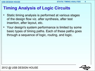
  • 4. Static timing analysis is performed at various stages of the design flow viz. after synthesis, after test insertion, after layout, etc. Your design's system performance is limited by some basic types of timing paths. Each of these paths goes through a sequence of logic, routing, and logic. Timing Analysis of Logic Circuits
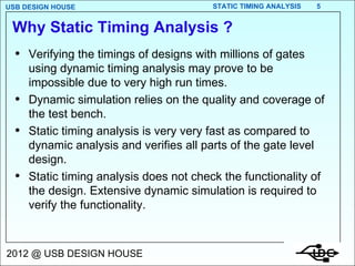
  • 5. Why Static Timing Analysis ? Verifying the timings of designs with millions of gates using dynamic timing analysis may prove to be impossible due to very high run times. Dynamic simulation relies on the quality and coverage of the test bench. Static timing analysis is very very fast as compared to dynamic analysis and verifies all parts of the gate level design. Static timing analysis does not check the functionality of the design. Extensive dynamic simulation is required to verify the functionality.
  • 6. Pad to Pad A pad-to-pad path starts at an input pad of the chip, propagates through one or more levels of combinational logic, and ends at an output pad of the chip. The pad-to-pad path time is the maximum time required for the data to enter the chip, travel through logic & routing, and leave the chip. It is not controlled or affected by any clock signal.
  • 8. Pad to Setup A pad-to-setup path starts at an input pad of the chip, propagates through input buffers and any number of combinatorial logic levels, and end at a D/T input to a flip-flop, latch or the receiving flip-flop’s t setup. Pad-to-set paths do not travel through flip-flops. The pad-to-setup path time is the maximum time required for the data to enter the chip, travel through logic and routing, and arrive at the input (D/T) before the clock or control signal arrives.
  • 10. Clock To Pad Paths A clock-to-pad path starts at a clock input of a flip-flop, propagates through the flip-flop Q output and any number of levels of combinatorial logic, and ends at an output pad. It includes the clock-to-Q delay (Tpff) of the flip-flop and the path delay from that flip-flop to the chip output. The clock-to-pad path time is the maximum time required for the data to leave the source flip-flop, travel through logic & routing, and leave the chip.
  • 11. Clock To Pad Paths
  • 12. Clock To Pad Through Tristates
  • 13. These are not valid clock to pad paths.
  • 14. Clock To Setup - Same Clock
  • 15. Rising Edge To Falling Edge Timing
  • 16. Falling Edge To Rising Edge
  • 17. Clock To Setup - Different Clocks
  • 18. The paths ending at the clock pin of other FFs or the asynchronous pins of other FFs are not valid clock to setup paths. Clock enable pins ? They are similar to data. They will also have setup requirement.
  • 19. Clock Pad To Clock Pin Of F/Fs
  • 20. E.g. 1 What is the minimum clock period (Tmin) for this circuit? Hint: Evaluate all FF to FF paths
  • 21. E.g. 1 contd. Path FFA to FFB TClk-Q(FFA) + Tpd(H) + Ts(FFB) = 5ns + 5ns+ 2ns = 12ns Path FFB to FFB TCLK-Q(FFB) + Tpd(F) + Tpd(H) + Ts(FFB) = 4ns + 4ns + 5ns + 2n = 15 ns So, Tmin=15 ns.
  • 22. E.g. 2 Analysis of All The Paths In The Circuit
  • 23. E.g. 2 Analysis of All The Paths In The Circuit Data at A, B, C and D is stable for 3 ns after the rising clock edge Data at X and Y has to be stable 3 ns before the rising clock edge. Calculate the maximum frequency of operation of the circuit. The delays are Tpd AND,OR= 1 ns, Tpd XOR= 2 ns, Tsetup= 1 ns, TclocktoQ = 3 ns.
  • 24. E.g. 2 contd. Pad to Pad A to Y: (i) Tin-G4-Tout = 3+1+3=7ns (ii) Tin-G1-G4-Tout = 3+1+1+3=8ns
  • 25. Pad to clock A-FF2D (i) Tin-G4-G7-TsetupFF2 =3+1+2+1=7ns (ii) Tin-G1-G4-G7-TsetupFF2 =3+1+1+2+1=8ns (iii) Tin-G5-G6-G7-TsetupFF2 =3+1+1+1+2+1=9ns C-FF2D: Tin-G3-G7-TsetupFF2 =3+1+2+1=7ns D-FF2D: Tin-G2-G5-G6-G7-TsetupFF2 =3+1+1+1+2+1=9ns C-FF2E Tin-G8-TsetupFF2 = 3+1+1=5ns D-FF2E Tin-G2-G5-G6-G8-TsetupFF2 =3+1+1+1+1+1=8ns
  • 26. Clock to clock path FF1D – FF2D: (i)Tclk-QFF1-G1-G4-G7-TsetupFF2 = 3+1+1+2+1 = 8ns (ii) Tclk-QFF1-G1-G5-G6-G7-TsetupFF2 = 3+1+1+1+2+1 = 9ns (iii) Tclk-QFF1-G2-G5-G6-G7-TsetupFF2 = 3+1+1+1+2+1 = 9ns (iv)Tclk-QnFF1-G6-G7-TsetupFF2 = 3+1+2+1 = 7ns (iv)Tclk-QnFF1-G3-G7-TsetupFF2 = 3+1+2+1 = 7ns
  • 27. Clock to clock path (contd.) FF1D – FF2E: (i) Tclk-QFF1-G1-G5-G6-G8-TsetupFF2 = 3+1+1+1+1+1 = 8ns (ii) Tclk-QFF1-G2-G5-G6-G8-TsetupFF2 = 3+1+1+1+1+1 = 8ns (iii)Tclk-QnFF1-G6-G8-TsetupFF2 = 3+1+1+1 = 6ns
  • 28. Clock to Pad FF1 – Y: (i) Tclk-QFF1-G1-G4-Tout = 3+1+1+3 = 8ns FF2 – X (i) Tclk-QFF2-Tout = 3+3 = 6ns Maximum period between clk to clk paths is 9 ns Maximum frequency of operation = 1/9 =111.11 Mhz