Fmax Analysis
1 like846 views
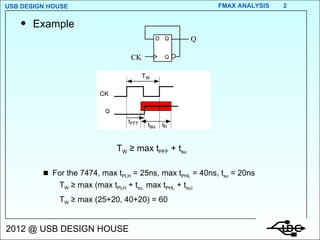
The maximum clock frequency for a synchronous sequential circuit is limited by the timing parameters of its flip-flops and gates. These parameters include propagation delays, setup times, and hold times. The minimum clock period is the reciprocal of the maximum clock frequency. For a specific 7474 circuit, the maximum clock period must be greater than or equal to 60 ns to account for the propagation delays and setup time of the flip-flops.
1 of 8


Recommended
Latch & Flip-Flop Design.pptx
Latch & Flip-Flop Design.pptxGargiKhanna2
Ěý
The document discusses latches and flip-flops. It describes how latches are used to store data values and are building blocks for master-slave flip-flops. It then discusses different types of latches including D latches, pass transistor latches, and static D latches. Various flip-flop designs are presented including using a pair of back-to-back latches and adding features like enables, resets, and sets. Transmission gate and precharge techniques are explored for building flip-flops with lower power consumption.Divide by N clock
Divide by N clockMantra VLSI
Ěý
this presentation is based to construct different frequency divide by clock with reference to the system clock.Timing Analysis
Timing Analysisrchovatiya
Ěý
The document discusses static timing analysis which is used to verify that logic circuits meet timing requirements. It analyzes different types of timing paths like pad-to-pad, pad-to-setup, clock-to-pad. Static timing analysis is preferred over dynamic analysis for verifying timings in large designs due to faster run times. An example shows calculating maximum frequency of operation by analyzing all path delays in a circuit.Vlsi(140083112008,15,16)
Vlsi(140083112008,15,16)Kashyap Mandaliya
Ěý
The document discusses various types of clocked latches and flip-flops. It describes the basic operation of a NOR-based SR latch and how adding a clock makes it level-sensitive. It also covers NAND-based SR latches, JK latches, master-slave flip-flops using NOR gates, and different implementations of D latches and D flip-flops using transmission gates or tri-state inverters. Timing considerations like setup and hold times are discussed for D latches. The document provides circuit schematics and truth tables for each circuit.Overview of SCTP (Stream Control Transmission Protocol)
Overview of SCTP (Stream Control Transmission Protocol)Peter R. Egli
Ěý
Overview of SCTP (Stream Control Transmission Protocol), outlining the main features and capabilities of SCTP.
SCTP is a transport protocol that overcomes many of the shortcomings of TCP, namely head-of-line blocking and stream-oriented transmission.
SCTP supports multiple streams within a connection and preserves boundaries of application messages thus greatly simplifying communication.
Additionally, SCTP supports multi-homing which increases availability in applications with high reliability demands.
SCTP inherits much of the congestion, flow and error control mechanisms of TCP.
SCTP has its roots in telecom carrier networks for use in transitional voice over IP scenarios.
However, SCTP is generic so that it is applicable in many enterprise applications as well.Setup and hold time violation in flip-flops
Setup and hold time violation in flip-flopsJong Hwan Shin
Ěý
When using a flip-flop, flip-flop should have constant input during setup time and hold time. This slide explains setup time violation and hold time violation in flip-flops.Delays in verilog
Delays in verilogJITU MISTRY
Ěý
Delays in Verilog allow modeling of timing aspects like propagation delays. There are different types of delays depending on the design approach - gate level modeling uses rise, fall, and turn-off delays while dataflow modeling uses assignment delays on nets. Behavioral modeling supports regular delays before assignments, intra-assignment delays after the equals sign, and zero delays to ensure last execution. Sequential and parallel blocks also control statement ordering.Synchronous and asynchronous clock
Synchronous and asynchronous clockNallapati Anindra
Ěý
The document discusses synchronous and asynchronous clocks. A clock is a square wave signal generated by an oscillator that provides two levels, high and low. Clocks are used to time signals in circuits to avoid glitches, which are unpredictable outputs caused by differences in propagation delays. There are two types of clocks: synchronous clocks have the same phase but frequencies may differ, while asynchronous clocks have different phases and frequencies may also differ. Asynchronous clocks can cause glitches, so synchronization is needed to make clocks operate synchronously.Pipelining approach
Pipelining approachGopinathD17
Ěý
This document discusses pipelining as an approach to optimize sequential circuits. It describes how pipelining can be implemented using registers between logic blocks to improve resource utilization and increase throughput. This allows computations to be spread over multiple clock cycles in an assembly-line fashion. The document also discusses latch-based vs register-based pipelines and different logic styles like NORA-CMOS that can be used for pipelined structures. It covers design rules and considerations for ensuring correct pipelined operation. Finally, it briefly describes non-bistable sequential circuits like astable, monostable and Schmitt trigger circuits.Metastability,MTBF,synchronizer & synchronizer failure
Metastability,MTBF,synchronizer & synchronizer failureprashant singh
Ěý
This document discusses metastability, mean time between failures (MTBF), synchronizers, and synchronizer failures. It begins with introductions to metastability and cases where it can occur. It then illustrates metastability with diagrams and graphs. It discusses how systems enter metastability and what occurs during metastability. The document derives the MTBF equation and provides an example calculation. It concludes by listing references for further information.Topograhical synthesis 
Topograhical synthesis Deiptii Das
Ěý
This document discusses topographical synthesis and its benefits. Topographical synthesis enables congestion prediction and avoidance early in the design flow during synthesis. It uses advanced optimization algorithms to deliver high quality results that correlate well to physical implementation. This eliminates costly iterations between synthesis and layout. Key benefits include accurately predicting congestion hotspots, performing optimizations to minimize congestion, and delivering results matched to post-layout timing and area without needing wire load models.design-compiler.pdf
design-compiler.pdfFrangoCamila
Ěý
Synthesis & gate-level simulation is introduced. The key topics covered include basic concepts of logic synthesis using Design Compiler, including logic level optimization, mapping, boundary optimization, and static timing analysis. Simulation of the gate-level netlist generated after synthesis is also discussed. An example lab is outlined to synthesize a simple 8-bit microprocessor and simulate the gate-level netlist.To designing counters using verilog code
To designing counters using verilog codeBharti Airtel Ltd.
Ěý
The document describes implementing up, down, and up/down counters using Verilog code. It includes:
1) Code for a 4-bit up counter that counts from 0 to 15 when the clock signal changes.
2) Code for a 4-bit down counter that counts from 15 to 0 when the clock signal changes.
3) Code for a 4-bit up/down counter that counts up when the up signal is high and down when the down signal is high, controlled by the clock.Verilog HDL Training Course
Verilog HDL Training CoursePaul Laskowski
Ěý
Verilog HDL (Hardware Description Language) Training Course for self-taught instructional. User should be familiar with basic digital and logic design. Helpful to have a Verilog simulator while going through examples.Timing analysis
Timing analysisKunal Doshi
Ěý
The paper describes the basic of Timing analysis like setup time, hold time, delays in logic circuits, timing violations and different types of timing paths like flip-flop to flip-flop path, clock gating path, asynchronous signal path, half cycle path, flip-flop to output path, input to flip-flop path and input to output path.Implementing Useful Clock Skew Using Skew Groups
Implementing Useful Clock Skew Using Skew GroupsM Mei
Ěý
Implementing useful skew through skew groups or manual buffer insertion can improve timing in a large memory block design. Skew groups define a target skew value for groups of clock pins before clock tree synthesis, resulting in a smaller clock tree, lower power increase, and less routing complexity compared to manual buffer insertion. Manual insertion precisely controls skew by adding buffers but dramatically increases clock cell count and power consumption versus skew groups. Both methods effectively improved setup timing for the memory block design.optimazation of standard cell layout
optimazation of standard cell layoutE ER Yash nagaria
Ěý
The document discusses various layout optimizations that can be made to standard cells to reduce both internal power and area. These include removing "hammer head" structures to decrease transistor length, moving gate contacts over active areas to reduce transistor height, and reducing source/drain capacitances to decrease dynamic current without impacting speed. Post-layout simulations showed a new D flip-flop design with these optimizations reduced internal power by 20% while maintaining clock-to-Q delay, and improved saturation current by 15-50% while reducing area by 20%.12 static timing_analysis_3_clocked_design
12 static timing_analysis_3_clocked_designUsha Mehta
Ěý
The document discusses concepts related to static timing analysis (STA) for clocked designs. It defines key timing terms like timing paths, clock skew, slack, and false paths. It explains that STA involves breaking a circuit into timing paths and calculating the delay of each path to check if timing constraints are met. Timing paths connect flip-flops and have startpoints and endpoints. Clock skew is the difference in latency for a clock signal to reach flip-flops. Slack is the difference between a path's required time and arrival time.13 static timing_analysis_4_set_up_and_hold_time_violation_remedy
13 static timing_analysis_4_set_up_and_hold_time_violation_remedyUsha Mehta
Ěý
The document discusses static timing analysis concepts including set-up time, hold time, timing violations, and techniques for fixing violations. It provides examples of how delays are considered in an ideal case without set-up/hold times versus cases with set-up/hold times. Methods for calculating maximum clock frequency and identifying violations are described. Ways to address violations including adjusting buffering, cell sizing, and placement are outlined. The role of static timing analysis in ASIC design flows is also summarized.Basics of Verilog.ppt
Basics of Verilog.pptCoEBMSITM
Ěý
The document provides an overview of Verilog HDL, including:
- Verilog HDL was invented in 1983/1984 and allows specification of digital systems at various levels of abstraction.
- It includes constructs for behavioral, algorithmic, register transfer, structural, and gate-level modeling.
- A basic Verilog module defines ports, data types, and functionality or structure. Modules can be instantiated as objects to build larger designs.
- The document outlines key Verilog concepts like modules, instances, data types, identifiers, keywords, and modeling approaches like behavioral and structural.Physical design-complete
Physical design-completeMurali Rai
Ěý
This document discusses various concepts related to physical design implementation. It describes the inputs and outputs of physical design tools, important checks to perform before starting design such as clock and high fanout net budgeting, and concepts like floorplanning, placement, routing, libraries, multi-voltage design, and clock tree synthesis and optimization.VLSI-Physical Design- Tool Terminalogy
VLSI-Physical Design- Tool TerminalogyMurali Rai
Ěý
The physical design flow begins with placement which involves assigning exact locations to modules like gates and standard cells to minimize area and interconnect cost while meeting timing constraints, with the goal of enabling easier routing; placement tools take as input the netlist, floorplan, libraries, and constraints to perform global and detailed placement as well as optimization. The quality of placement significantly impacts the ability to route the design successfully.Basic synthesis flow and commands in digital VLSI
Basic synthesis flow and commands in digital VLSISurya Raj
Ěý
This document discusses logic synthesis, including the basic synthesis flow and commands, synthesis script flow, technology libraries, design objects like cells and ports, timing paths, and constraints like defining clocks and input/output delays. It provides examples of setting library variables, reading and writing designs, and applying constraints to clocks and I/O. The document contains information on synthesis tools and processes at a high level.sta slide ref.pdf
sta slide ref.pdfquandao25
Ěý
This document provides an overview of sequential clocking and static timing analysis for digital VLSI design. It discusses key timing parameters for sequential elements like setup time and hold time. It also explains how static timing analysis works by calculating arrival times and required arrival times for all nodes to find timing violations. The document notes that while static timing analysis is useful, it cannot analyze all timing issues and may report false paths. An example is provided to illustrate how arrival times, required arrival times and slack are calculated for a simple circuit. Finally, it mentions that design constraints must be specified to inform the timing analysis of requirements.VLSIM11.pptx
VLSIM11.pptxsavithaj5
Ěý
This document provides an overview of VLSI design. It begins with definitions of integrated circuits, VLSI, MOS and CMOS. It then discusses the evolution of transistors from vacuum tubes to MOSFETs. Key developments included the first transistor in 1947, first integrated circuit in 1958 using bipolar junction transistors, and introduction of MOSFETs and CMOS logic in 1960-1963. The document covers Moore's Law, decreasing feature sizes, logic gates, pass transistors, multiplexers, latches, flip-flops and their implementations in CMOS technology. It provides circuit diagrams and explanations of various digital building blocks used in VLSI systems.Pd flow i
Pd flow iAlok Kumar
Ěý
1. The document discusses the key steps in physical design flow, including import design, floorplanning, placement and routing.
2. Floorplanning is described as a critical step, where the quality of the floorplan can significantly impact timing closure and design implementation. Good techniques for floorplanning include understanding the design requirements and data flow.
3. The document outlines the major steps in floorplanning such as sizing and shaping blocks, voltage area creation, pin placement, row creation, macro placement, adding blockages and special cells. Qualifying the floorplan involves checks on pin grids, design rules, power connections and more.Verilog Lecture4 2014
Verilog Lecture4 2014BĂ©o TĂş
Ěý
This document discusses behavioral Verilog coding constructs including always and initial blocks, blocking vs non-blocking assignments, and if-else and case statements. It provides examples of coding flip-flops and sequential logic using these constructs. It also discusses simulator mechanics and the stratified event queue model of simulation.SPEF format
SPEF formatVLSI SYSTEM Design
Ěý
So, this has been due for long time. May be because of tight tape out deadlines, this very important piece of Physical Design flow just got missed. And I am sure, like me, many might be curious to know what is the IEEE SPEF format, what does various attributes of SPEF file represent, etc...
Clock Skew 1
Clock Skew 1rchovatiya
Ěý
Clock skew refers to the difference in arrival times of a clock signal at different devices. Excessive clock skew can be minimized by buffering the clock signal so that all signals experience equal delays, adding delay to the data path to account for skew, reversing the clock signal direction to clock the destination register before the source, or using alternate phase clocking with two clock phases or opposite clock edges between sequential registers.Metastability
MetastabilityNallapati Anindra
Ěý
Flip-flops can enter a metastable state where the output oscillates between 0 and 1 if setup and hold times are violated, such as with asynchronous signals, skewed clocks between domains, or changing inputs in the critical timing window. To resolve metastability, the flip-flop output will eventually settle to a stable 0 or 1 state, though the time to resolve can vary by technology. Cascading multiple flip-flops can help avoid metastable states.More Related Content
What's hot (20)
Pipelining approach
Pipelining approachGopinathD17
Ěý
This document discusses pipelining as an approach to optimize sequential circuits. It describes how pipelining can be implemented using registers between logic blocks to improve resource utilization and increase throughput. This allows computations to be spread over multiple clock cycles in an assembly-line fashion. The document also discusses latch-based vs register-based pipelines and different logic styles like NORA-CMOS that can be used for pipelined structures. It covers design rules and considerations for ensuring correct pipelined operation. Finally, it briefly describes non-bistable sequential circuits like astable, monostable and Schmitt trigger circuits.Metastability,MTBF,synchronizer & synchronizer failure
Metastability,MTBF,synchronizer & synchronizer failureprashant singh
Ěý
This document discusses metastability, mean time between failures (MTBF), synchronizers, and synchronizer failures. It begins with introductions to metastability and cases where it can occur. It then illustrates metastability with diagrams and graphs. It discusses how systems enter metastability and what occurs during metastability. The document derives the MTBF equation and provides an example calculation. It concludes by listing references for further information.Topograhical synthesis
Topograhical synthesis Deiptii Das
Ěý
This document discusses topographical synthesis and its benefits. Topographical synthesis enables congestion prediction and avoidance early in the design flow during synthesis. It uses advanced optimization algorithms to deliver high quality results that correlate well to physical implementation. This eliminates costly iterations between synthesis and layout. Key benefits include accurately predicting congestion hotspots, performing optimizations to minimize congestion, and delivering results matched to post-layout timing and area without needing wire load models.design-compiler.pdf
design-compiler.pdfFrangoCamila
Ěý
Synthesis & gate-level simulation is introduced. The key topics covered include basic concepts of logic synthesis using Design Compiler, including logic level optimization, mapping, boundary optimization, and static timing analysis. Simulation of the gate-level netlist generated after synthesis is also discussed. An example lab is outlined to synthesize a simple 8-bit microprocessor and simulate the gate-level netlist.To designing counters using verilog code
To designing counters using verilog codeBharti Airtel Ltd.
Ěý
The document describes implementing up, down, and up/down counters using Verilog code. It includes:
1) Code for a 4-bit up counter that counts from 0 to 15 when the clock signal changes.
2) Code for a 4-bit down counter that counts from 15 to 0 when the clock signal changes.
3) Code for a 4-bit up/down counter that counts up when the up signal is high and down when the down signal is high, controlled by the clock.Verilog HDL Training Course
Verilog HDL Training CoursePaul Laskowski
Ěý
Verilog HDL (Hardware Description Language) Training Course for self-taught instructional. User should be familiar with basic digital and logic design. Helpful to have a Verilog simulator while going through examples.Timing analysis
Timing analysisKunal Doshi
Ěý
The paper describes the basic of Timing analysis like setup time, hold time, delays in logic circuits, timing violations and different types of timing paths like flip-flop to flip-flop path, clock gating path, asynchronous signal path, half cycle path, flip-flop to output path, input to flip-flop path and input to output path.Implementing Useful Clock Skew Using Skew Groups
Implementing Useful Clock Skew Using Skew GroupsM Mei
Ěý
Implementing useful skew through skew groups or manual buffer insertion can improve timing in a large memory block design. Skew groups define a target skew value for groups of clock pins before clock tree synthesis, resulting in a smaller clock tree, lower power increase, and less routing complexity compared to manual buffer insertion. Manual insertion precisely controls skew by adding buffers but dramatically increases clock cell count and power consumption versus skew groups. Both methods effectively improved setup timing for the memory block design.optimazation of standard cell layout
optimazation of standard cell layoutE ER Yash nagaria
Ěý
The document discusses various layout optimizations that can be made to standard cells to reduce both internal power and area. These include removing "hammer head" structures to decrease transistor length, moving gate contacts over active areas to reduce transistor height, and reducing source/drain capacitances to decrease dynamic current without impacting speed. Post-layout simulations showed a new D flip-flop design with these optimizations reduced internal power by 20% while maintaining clock-to-Q delay, and improved saturation current by 15-50% while reducing area by 20%.12 static timing_analysis_3_clocked_design
12 static timing_analysis_3_clocked_designUsha Mehta
Ěý
The document discusses concepts related to static timing analysis (STA) for clocked designs. It defines key timing terms like timing paths, clock skew, slack, and false paths. It explains that STA involves breaking a circuit into timing paths and calculating the delay of each path to check if timing constraints are met. Timing paths connect flip-flops and have startpoints and endpoints. Clock skew is the difference in latency for a clock signal to reach flip-flops. Slack is the difference between a path's required time and arrival time.13 static timing_analysis_4_set_up_and_hold_time_violation_remedy
13 static timing_analysis_4_set_up_and_hold_time_violation_remedyUsha Mehta
Ěý
The document discusses static timing analysis concepts including set-up time, hold time, timing violations, and techniques for fixing violations. It provides examples of how delays are considered in an ideal case without set-up/hold times versus cases with set-up/hold times. Methods for calculating maximum clock frequency and identifying violations are described. Ways to address violations including adjusting buffering, cell sizing, and placement are outlined. The role of static timing analysis in ASIC design flows is also summarized.Basics of Verilog.ppt
Basics of Verilog.pptCoEBMSITM
Ěý
The document provides an overview of Verilog HDL, including:
- Verilog HDL was invented in 1983/1984 and allows specification of digital systems at various levels of abstraction.
- It includes constructs for behavioral, algorithmic, register transfer, structural, and gate-level modeling.
- A basic Verilog module defines ports, data types, and functionality or structure. Modules can be instantiated as objects to build larger designs.
- The document outlines key Verilog concepts like modules, instances, data types, identifiers, keywords, and modeling approaches like behavioral and structural.Physical design-complete
Physical design-completeMurali Rai
Ěý
This document discusses various concepts related to physical design implementation. It describes the inputs and outputs of physical design tools, important checks to perform before starting design such as clock and high fanout net budgeting, and concepts like floorplanning, placement, routing, libraries, multi-voltage design, and clock tree synthesis and optimization.VLSI-Physical Design- Tool Terminalogy
VLSI-Physical Design- Tool TerminalogyMurali Rai
Ěý
The physical design flow begins with placement which involves assigning exact locations to modules like gates and standard cells to minimize area and interconnect cost while meeting timing constraints, with the goal of enabling easier routing; placement tools take as input the netlist, floorplan, libraries, and constraints to perform global and detailed placement as well as optimization. The quality of placement significantly impacts the ability to route the design successfully.Basic synthesis flow and commands in digital VLSI
Basic synthesis flow and commands in digital VLSISurya Raj
Ěý
This document discusses logic synthesis, including the basic synthesis flow and commands, synthesis script flow, technology libraries, design objects like cells and ports, timing paths, and constraints like defining clocks and input/output delays. It provides examples of setting library variables, reading and writing designs, and applying constraints to clocks and I/O. The document contains information on synthesis tools and processes at a high level.sta slide ref.pdf
sta slide ref.pdfquandao25
Ěý
This document provides an overview of sequential clocking and static timing analysis for digital VLSI design. It discusses key timing parameters for sequential elements like setup time and hold time. It also explains how static timing analysis works by calculating arrival times and required arrival times for all nodes to find timing violations. The document notes that while static timing analysis is useful, it cannot analyze all timing issues and may report false paths. An example is provided to illustrate how arrival times, required arrival times and slack are calculated for a simple circuit. Finally, it mentions that design constraints must be specified to inform the timing analysis of requirements.VLSIM11.pptx
VLSIM11.pptxsavithaj5
Ěý
This document provides an overview of VLSI design. It begins with definitions of integrated circuits, VLSI, MOS and CMOS. It then discusses the evolution of transistors from vacuum tubes to MOSFETs. Key developments included the first transistor in 1947, first integrated circuit in 1958 using bipolar junction transistors, and introduction of MOSFETs and CMOS logic in 1960-1963. The document covers Moore's Law, decreasing feature sizes, logic gates, pass transistors, multiplexers, latches, flip-flops and their implementations in CMOS technology. It provides circuit diagrams and explanations of various digital building blocks used in VLSI systems.Pd flow i
Pd flow iAlok Kumar
Ěý
1. The document discusses the key steps in physical design flow, including import design, floorplanning, placement and routing.
2. Floorplanning is described as a critical step, where the quality of the floorplan can significantly impact timing closure and design implementation. Good techniques for floorplanning include understanding the design requirements and data flow.
3. The document outlines the major steps in floorplanning such as sizing and shaping blocks, voltage area creation, pin placement, row creation, macro placement, adding blockages and special cells. Qualifying the floorplan involves checks on pin grids, design rules, power connections and more.Verilog Lecture4 2014
Verilog Lecture4 2014BĂ©o TĂş
Ěý
This document discusses behavioral Verilog coding constructs including always and initial blocks, blocking vs non-blocking assignments, and if-else and case statements. It provides examples of coding flip-flops and sequential logic using these constructs. It also discusses simulator mechanics and the stratified event queue model of simulation.SPEF format
SPEF formatVLSI SYSTEM Design
Ěý
So, this has been due for long time. May be because of tight tape out deadlines, this very important piece of Physical Design flow just got missed. And I am sure, like me, many might be curious to know what is the IEEE SPEF format, what does various attributes of SPEF file represent, etc...
Viewers also liked (6)
Clock Skew 1
Clock Skew 1rchovatiya
Ěý
Clock skew refers to the difference in arrival times of a clock signal at different devices. Excessive clock skew can be minimized by buffering the clock signal so that all signals experience equal delays, adding delay to the data path to account for skew, reversing the clock signal direction to clock the destination register before the source, or using alternate phase clocking with two clock phases or opposite clock edges between sequential registers.Metastability
MetastabilityNallapati Anindra
Ěý
Flip-flops can enter a metastable state where the output oscillates between 0 and 1 if setup and hold times are violated, such as with asynchronous signals, skewed clocks between domains, or changing inputs in the critical timing window. To resolve metastability, the flip-flop output will eventually settle to a stable 0 or 1 state, though the time to resolve can vary by technology. Cascading multiple flip-flops can help avoid metastable states.Metastability
Metastabilityrchovatiya
Ěý
Metastability occurs when the inputs to a flip-flop violate the setup and hold timing requirements around the clock edge. This can cause the output to momentarily exist in an unstable intermediate state between logic 0 and 1. The likelihood of metastability increases when asynchronous inputs are sampled by a synchronous system. Well-designed synchronizers use multiple flip-flops in series to resolve metastability within the clock period and avoid failures. The mean time between synchronizer failures depends on factors like clock speed and input transition rate.Clock Skew 2
Clock Skew 2rchovatiya
Ěý
Clock skew refers to differences in the arrival times of a clock signal at different flip-flops. Clock skew is caused by differences in delays along the paths from the clock generator to each flip-flop due to factors like wire lengths, gates, and clock edge inversion. The amount of clock skew affects calculations for the maximum clock frequency and allowable clock skew depends on the minimum setup and hold times of the flip-flops.I2C
I2Crchovatiya
Ěý
I2C is a serial communication protocol used to connect low-speed peripherals to processors and microcontrollers. It was developed by Philips in the 1980s for use in televisions. I2C uses just two bidirectional open-drain lines: serial data line (SDA) and serial clock line (SCL). Devices can operate as master or slave devices and have a 7-bit address. Communication is initiated by the master which controls the clock signal. Data is transferred in one byte packets with acknowledgement from the receiver.Career Development Quotes
Career Development QuotesAntoinette Oglethorpe
Ěý
25 Inspirational Quotes to help employees take ownership of their career development in your organisation.
Is your talent development strategy working? Learn how to increase your competitive advantage; engage, retain and develop your best people; and save serious amounts of time and money.
Download your FREE Talent development Audit at http://www.antoinetteoglethorpe.com/talent-development-audit/
Fmax Analysis
- 1. Maximum Clock Frequency The clock frequency for a synchronous sequential circuit is limited by the timing parameters of its flip-flops and gates. This limit is called the maximum clock frequency for the circuit. The minimum clock period is the reciprocal of this frequency. Relevant timing parameters Gates: Propagation delays: min t PLH , min t PHL , max t PLH , max t PHL Flip-Flops: Propagation delays: min t PLH , min t PHL , max t PLH , max t PHL Setup time: t su Hold time: t h
- 2. Example T W ≥ max t PFF + t su For the 7474, max t PLH = 25ns, max t PHL = 40ns, t su = 20ns T W ≥ max (max t PLH + t su, max t PHL + t su) T W ≥ max (25+20, 40+20) = 60
- 3. Example T W ≥ max t PFF + max t PINV + t su
- 4. Example T W ≥ max t PFF + max t PMUX + t su
- 5. Example Paths from Q1 to Q1: Paths from Q1 to Q2: Paths from Q2 to Q1: Paths from Q2 to Q2: None T W ≥ max t PDFF +t JKsu = 20 +10 = 30 ns T W ≥ max t PDFF + max t AND + t JKsu = 20 + 12 + 10 = 42 ns T W ≥ max t PJKFF + t OR + T Dsu = 25 + 10 + 5 = 40 ns T W ≥ max t PJKFF + max t AND + t JKsu = 25 + 12 + 10 = 47 ns TW ≥ 47 ns
- 6. Example T W ≥ max t PFF + max t PINV + t su
- 7. Example T W ≥ max t PFF + max t PMUX + t su
- 8. Example Paths from Q1 to Q1: Paths from Q1 to Q2: Paths from Q2 to Q1: Paths from Q2 to Q2: None T W ≥ max t PDFF +t JKsu = 20 +10 = 30 ns T W ≥ max t PDFF + max t AND + t JKsu = 20 + 12 + 10 = 42 ns T W ≥ max t PJKFF + t OR + T Dsu = 25 + 10 + 5 = 40 ns T W ≥ max t PJKFF + max t AND + t JKsu = 25 + 12 + 10 = 47 ns TW ≥ 47 ns