尝迟蝉辫颈肠别を活用したトランシ?スタの基本特性シミュレーション
Download as PPTX, PDF0 likes12,188 views

回路シミュレーションサービスを提供するマルツエレックのSPICE入門講座。LTspiceを活用したトランジスタの基本特性シミュレーションの資料です。 http://www.marutsu.co.jp/ キーワード:Ic-hFE特性、飽和電圧特性、スイッチング特性


![飽和電圧特性
VBE(sat)=850.692m[V]
VCE(sat)=323.778m[V]
シミュレーション結果
Copyright(C) MARUTSU ELEC CO. LTD 6](https://image.slidesharecdn.com/ltspice-141028185144-conversion-gate02/85/Ltspice-6-320.jpg)
![スイッチング特性
Data Sheetの測定条件
Ic=2.5[A]
IB1=0.5[A]
IB2=1[A]
RL=60[Ω]
VBB2=4[V]
VBB Vbe sat
2 ( )
2
4 0.85
1
IB
RB
RB
?
?
?
?
RB=4.85[Ω]
①ベース抵抗RBの値を決定する
②VPULSEの条件を決定する
VBB Vbe sat
1 ( )
1
1 0.85
0.5
4.85
IB
RB
VBB
?
?
?
?
VBB1=3.275[V]
Copyright(C) MARUTSU ELEC CO. LTD 7](https://image.slidesharecdn.com/ltspice-141028185144-conversion-gate02/85/Ltspice-7-320.jpg)

![スイッチング特性
IB1=0.5[A]
シミュレーション結果
IB2=1.0[A]
Copyright(C) MARUTSU ELEC CO. LTD 9](https://image.slidesharecdn.com/ltspice-141028185144-conversion-gate02/85/Ltspice-9-320.jpg)


More Related Content
Similar to 尝迟蝉辫颈肠别を活用したトランシ?スタの基本特性シミュレーション (20)
More from マルツエレック株式会社 marutsuelec (20)


尝迟蝉辫颈肠别を活用したトランシ?スタの基本特性シミュレーション
- 1. LTspiceを活用した トランジスタの基本特性シミュレーション Ic-hFE特性 飽和電圧特性 スイッチング特性 1 2014年10月24日 マルツエレック株式会社 Copyright(C) MARUTSU ELEC CO. LTD
- 2. 2 トランジスタのSPICEモデルについて トランジスタのSPICEモデルには幾つかの種類があります。 エバースモルモデルとガンメルプーンモデルです。エバースモルモデル はモデルが古く、現在では、フォトカプラ、フォトICのトランジスタ表現に 採用されているくらいであり、ガンメルプーンモデルが主流です。今回の トランジスタのSPICEモデルもガンメルプーンモデルを採用しています。 トランジスタのデバイスモデリング教材について ガンメルプーンモデルをPSpice Model Editorを使用したデバイス モデリングの教材をご提供しています。是非、ご活用下さい。各電気 的特性とパラメータモデルの関連性も記載されているので、LTspiceで もパラメトリック解析にてデバイスモデリング可能です。 トランジスタのデバイスモデリング教材についての詳細情報は 下記のURLでご確認下さい。 http://www.marutsu.co.jp/pc/i/130715/ Copyright(C) MARUTSU ELEC CO. LTD
- 3. Ic-hFE特性 評価回路図 Copyright(C) MARUTSU ELEC CO. LTD 3
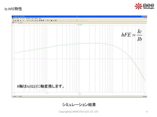
- 4. Ic-hFE特性 シミュレーション結果 Ic hFE Ib ? X軸はIc(Q1)に軸変換します。 Copyright(C) MARUTSU ELEC CO. LTD 4
- 5. 飽和電圧特性 評価回路図 Copyright(C) MARUTSU ELEC CO. LTD 5
- 6. 飽和電圧特性 VBE(sat)=850.692m[V] VCE(sat)=323.778m[V] シミュレーション結果 Copyright(C) MARUTSU ELEC CO. LTD 6
- 7. スイッチング特性 Data Sheetの測定条件 Ic=2.5[A] IB1=0.5[A] IB2=1[A] RL=60[Ω] VBB2=4[V] VBB Vbe sat 2 ( ) 2 4 0.85 1 IB RB RB ? ? ? ? RB=4.85[Ω] ①ベース抵抗RBの値を決定する ②VPULSEの条件を決定する VBB Vbe sat 1 ( ) 1 1 0.85 0.5 4.85 IB RB VBB ? ? ? ? VBB1=3.275[V] Copyright(C) MARUTSU ELEC CO. LTD 7
- 8. スイッチング特性 評価回路図 Copyright(C) MARUTSU ELEC CO. LTD 8
- 9. スイッチング特性 IB1=0.5[A] シミュレーション結果 IB2=1.0[A] Copyright(C) MARUTSU ELEC CO. LTD 9
- 10. Appendix A トランジスタのSPICEモデル トランジスタは、新電元工業製品の「2SC4054 」を採用した。Gummel-Poonモデル であり、順逆方向特性に再現性のある解析精度の高いSPICEモデルである。 *$ * PART NUMBER: 2SC4054 * MANUFACTURER: SHINDENGEN * All Rights Reserved Copyright (C) Bee Technologies Inc. 2004 .MODEL Q2SC4054 NPN + IS=2.4201E-12 BF=92.371 VAF=44.700 + IKF=4.5256 ISE=5.4332E-12 NE=1.2547 + BR=3.2573 VAR=1.8738 IKR=20 + ISC=11.004E-9 NC=1.8738 NK=.65071 + RB=.16891 RC=95.122E-3 CJE=2.2596E-9 + VJE=.53979 MJE=.30943 CJC=321.38E-12 + VJC=.53259 MJC=.4805 TF=21.000E-9 + XTF=10 VTF=10 ITF=1 + TR=427.00E-9 *$ Copyright(C) MARUTSU ELEC CO. LTD 10
- 11. Appendix B シミュレーションデータの格納先 Ic-hFE特性 飽和電圧特性 スイッチング特性 Copyright(C) MARUTSU ELEC CO. LTD 11